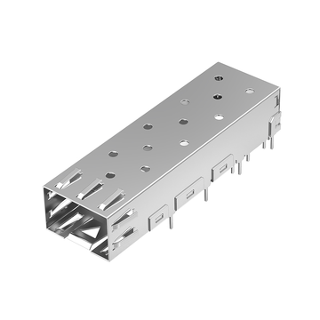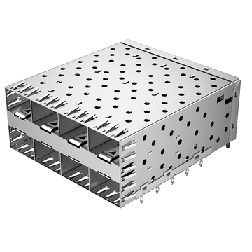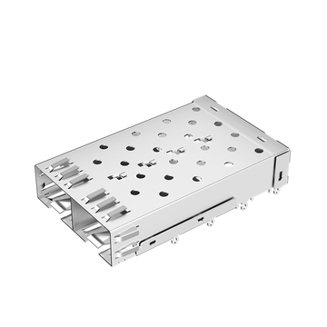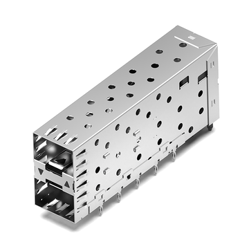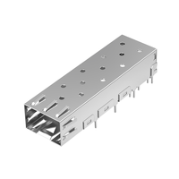
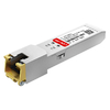
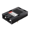
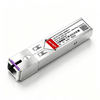
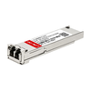
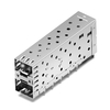
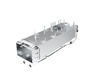
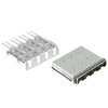

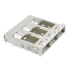

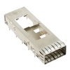
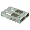
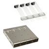




Haben Sie schon einmal einen SFP-Käfig oder High-Speed-SFP+-Käfige in ein neues Platinenlayout integriert, die MSA-Standards strikt eingehalten und dennoch unerwartete Montage- oder Signalintegritätsfehler festgestellt? Spezifikationen wie SFF-8432 definieren zwar grundlegende Abmessungen und Steckregeln, berücksichtigen aber selten die realen Belastungen moderner Netzwerkhardware. Wenn hochdichte Layouts die Bauteilgrenzen ausreizen, bleiben kritische Hardware-Schwachstellen oft ungelöst, wenn man sich ausschließlich auf die MSA-Standards verlässt.
Warum kommt es bei scheinbar konformen Designs dennoch zu elektromagnetischen Störungen, Bauteilüberhitzung oder beschädigten Durchkontaktierungen auf der Leiterplatte während der Fertigung? Die Antwort liegt in den subtilen mechanischen Toleranzen, die in der Standarddokumentation dem Ermessen des Herstellers überlassen werden. Die Bewertung von Faktoren wie dem Halt der Befestigungsstifte, den Kräften der Kühlkörperklammern, der Federkraft der Lünette und der Anordnung der Anschlüsse übereinander macht den entscheidenden Unterschied zwischen einem fehlgeschlagenen Prototyp und einer robusten Serienproduktion aus.
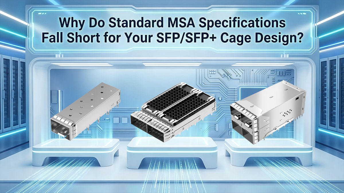
🔷 Warum reichen die Standard-MSA-Spezifikationen für Ihr SFP/SFP+-Käfigdesign nicht aus?
Branchenweite Multi-Source-Agreements (MSAs) legen die mechanischen Grundvoraussetzungen fest, um die physische Austauschbarkeit von Hardware verschiedener Hersteller zu gewährleisten. Die Einhaltung von Standards allein garantiert jedoch keine zuverlässige Leistung unter Hochgeschwindigkeitsbedingungen und starker physikalischer Belastung. Für eine erfolgreiche Integration müssen Hardware-Ingenieure kritische elektromechanische Parameter bewerten, die weit über die Standard-Grenzflächenzeichnungen hinausgehen.
Geltungsbereich und Grenzen der SFF-8432-Spezifikationen
Die SFF-8432-Spezifikation definiert primär die äußeren Abmessungen des Gehäuses, den Portabstand und die grundlegende Geometrie der Gehäuseausschnitte. Diese Definitionen gewährleisten, dass jedes Standardmodul mit einem SFP- oder SFP+-Gehäuse eines unabhängigen Herstellers kompatibel ist.
Der Standard überlässt jedoch bewusst fertigungskritische Details – wie z. B. Presspassungsstiftprofile, Wärmeleitschnittstellen und Federsteifigkeit – dem Ermessen der Hersteller. Dies zwingt Systementwickler, diese Parameter bei der Komponentenauswahl eigenständig zu überprüfen, anstatt sich allein auf die MSA-Konformität zu verlassen.
Mechanische Belastung in der Praxis vs. Basisnachgiebigkeit
Die MSA-Konformitätsprüfung bestätigt die statische Passgenauigkeit, Netzwerkhardware ist jedoch während ihres gesamten Lebenszyklus dynamischen mechanischen Belastungen ausgesetzt. Wiederholtes Einstecken von Transceivern, Wärmeausdehnung bei hoher Last und Gehäuseflexibilität erzeugen kontinuierliche Spannungen an der Leiterplattenschnittstelle.
Ohne Berücksichtigung der strukturellen Stabilität und des Pin-Haltes kann der kontinuierliche Modulwechsel die Befestigungslaschen eines SFP/SFP+-Käfigs lockern. Mit der Zeit führt diese mechanische Ermüdung zu einer Verschlechterung der Masseverbindung und zur Beschädigung empfindlicher Verbindungen auf der Platine.
Häufige Fehler bei der Leiterplattenbestückung – über die grundlegenden Abmessungen hinaus.
Standardmäßige technische Zeichnungen berücksichtigen selten die engen Fertigungstoleranzen, die für moderne Leiterplatten erforderlich sind. Geringfügige Abweichungen zwischen den Nennmaßen der Pins und den Beschichtungen der Bohrungen können beim Einpressen zu Leiterbahnbrüchen oder Ablösungen der Ringschichten führen.
Ähnlich verhält es sich mit SMD-Lötprozessen: Lötbrücken oder unvollständige Benetzung treten häufig auf, wenn die Koplanarität der Käfigstifte geringfügig von der Platinenebene abweicht. Die frühzeitige Berücksichtigung dieser Maßabweichungen verhindert hohe Ausschussquoten und geringe Produktionsausbeuten bei der Serienfertigung.
Auswirkungen der kundenspezifischen Chassis-Integration auf die Toleranzanalyse
Der Einsatz eines SFP- oder SFP+-Käfigs in realen Unternehmensswitches erfordert eine präzise Ausrichtung mit den kundenspezifischen Frontblenden und Abdeckplatten. Durch die Fertigungstoleranzen des Blechgehäuses, der Abstandshalter des Motherboards und des Käfigkörpers kommt es häufig zu mechanischen Störungen.
Selbst geringfügige Stapelfehler können dazu führen, dass der Modulverriegelungsmechanismus klemmt und ein reibungsloses Einsetzen des Transceivers verhindert. Eine präzise mechanische Modellierung gewährleistet, dass der Käfig bei allen Fertigungstoleranzen korrekt in der Blendenöffnung zentriert bleibt.
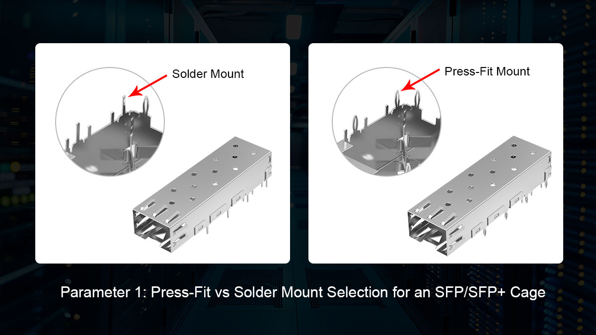
🔷 Parameter 1: Auswahl zwischen Press-Fit- und Lötmontage für einen SFP/SFP+-Käfig
Die zuverlässige Befestigung der Käfigbaugruppe auf der Leiterplatte ist der grundlegende Schritt, um Beschädigungen empfindlicher Hochgeschwindigkeitsleiterbahnen durch mechanische Belastung zu vermeiden. Die Wahl zwischen Press- und Lötmontage definiert die physikalischen Rahmenbedingungen für die Leiterplattenfertigung, die Montageanlagen und die allgemeine Zuverlässigkeit im Feldeinsatz. Die Wahl der falschen Anschlussmethode kann Hochfrequenzsignalwege beeinträchtigen und bei kontinuierlichen Transceiver-Einsteckzyklen zu vorzeitiger Materialermüdung führen.
Einpress-Nadelstifte vs. Lötstiftbaugruppe
Presspassungsverbindungen nutzen nachgiebige Nadelöhr-Stifte, die sich beim Einpressen in durchkontaktierte Löcher elastisch verformen und so eine luftdichte mechanische und elektrische Verbindung ohne thermische Belastung herstellen. Lötmontagen hingegen basieren auf Wellenlöt- oder Reflow-Lötverfahren zur Befestigung starrer Stifte auf Leiterplattenflächen und eignen sich daher für Anwendungen mit geringerer Beanspruchung.
Die strukturellen und verarbeitungstechnischen Unterschiede zwischen diesen beiden Befestigungsarten verdeutlichen deutliche technische Kompromisse:
| Parameter / Funktion | Presspassung (nachgiebiger Stift) | Lötmontage (SMT / Durchsteckmontage) |
| Montagemechanismus | Mechanische Presspassung durch Stiftverformung | Metallurgische Lötverbindung |
| Thermische Belastung | Keine (Kaltmontageverfahren) | Hohe Reflow- oder Wellenlöttemperaturen |
| Mechanische Retention | Hohe Beständigkeit gegenüber wiederholter Einführbelastung | Geringerer Widerstand gegen anhaltende Scherspannung |
| Auswirkungen des Leiterplattenlayouts | Erfordert Durchgangslöcher mit dicker Kupferoberfläche | Erfordert Oberflächenpads oder Durchgangslöcher. |
| Werkzeugabhängigkeit | Hochpräzise Presspassungs-Sitzvorrichtungen | Standard-Schablonen-, Reflow-Ofen- oder Wellenanlagen |
Einfügekraft vs. thermische Lötgrenzen
Für die Presspassung ist eine präzise dosierte Einpresskraft erforderlich, um den SFP/SFP+-Käfig vollständig auf dem Motherboard zu fixieren, ohne das hohle Blechgehäuse zu beschädigen. Wird die empfohlene Einpresskraft überschritten, besteht die Gefahr, dass sich die Leiterplatte verbiegt, interne Masseflächen beschädigt oder interne Transceiver-Führungsschienen verformt werden.
Lötkäfige umgehen zwar die mechanischen Presskräfte, setzen aber die umliegenden Layoutbereiche erhöhten Reflow-Temperaturen aus. Wiederholte Temperaturzyklen können zu lokalen Verformungen des Substrats führen, was wiederum intermittierende Unterbrechungen oder Risse in den Lötstellen benachbarter Hochgeschwindigkeits-Differenzsignalleitungen zur Folge haben kann.
Toleranzen für Leiterplattenlöcher im Vergleich zu den Anforderungen an das Pad-Layout
Bei der Herstellung hochdichter Leiterplatten für SFP- oder Multiport-SFP+-Gehäuse ist eine präzise Fertigungssteuerung unerlässlich. Da Presspassungsstifte auf der radialen Ausdehnung gegen die Gehäusewände beruhen, während Lötstifte präzise metallurgische Randbedingungen erfordern, ergeben sich für jede Technologie spezifische Regeln für das Leiterplattenlayout.
Eine sorgfältige Prüfung der folgenden Layoutvorgaben gewährleistet eine reibungslose Fertigung:
- Fertiger Bohrungsdurchmesser: Die Toleranzen für Presspassungsbohrungen müssen strikt +/-0.05 mm betragen.
- Beschichtungsdicke: Um ein Aufreißen der Wand beim Einführen des Stifts zu vermeiden, muss die Kupferbeschichtung des Zylinders mindestens 25µm dick sein.
- Integrität des Rings: Ausreichende Kupferringränder gewährleisten, um ein Durchbrechen unter mechanischer Scherung zu verhindern.
- Pin-in-Paste (PIP) Lochfüllung: Lötdurchgangslöcher genau dimensionieren, um beim Reflow eine vertikale Lötmittelfüllung von mindestens 75 % zu erreichen.
- Schablonenöffnung & Pastenvolumen: Optimieren Sie die SMT-Schablonenöffnungsverhältnisse, um Lötbrücken zu vermeiden und gleichzeitig eine ausreichende Kehlnahthöhe zu gewährleisten.
- Abstand der Lötstoppmasken-Dämme: Sorgen Sie für ausreichend große Lötstoppmasken-Dämme um dichte Masseflächen, um Flussmitteleinschlüsse und Kurzschlüsse zu vermeiden.
Einfache Reparatur und Überarbeitung für beide Montagearten
Die Wartungsfreundlichkeit im Feld und die Arbeitsabläufe für Nacharbeiten in der Fertigung unterscheiden sich zwischen diesen beiden Montagearten erheblich. Das Entlöten eines mehrpoligen Durchsteckkäfigs erfordert spezielle Heißluft-Entlötwerkzeuge und eine längere Hitzeeinwirkung, wodurch häufig benachbarte empfindliche Transceiver-Treiber-ICs beschädigt oder Kunststoff-Lichtleiterkomponenten geschmolzen werden.
Presspassungsbaugruppen ermöglichen eine saubere mechanische Entnahme mithilfe spezieller Ausziehvorrichtungen, die einen gleichmäßigen Druck nach oben auf die unteren Laschen ausüben. Allerdings halten einzelne Leiterplattenlöcher in der Regel nur zwei bis drei Austauschzyklen stand, bevor der Verschleiß der Kupferwände die Haltekraft unter die zulässigen Betriebssicherheitsgrenzen reduziert.
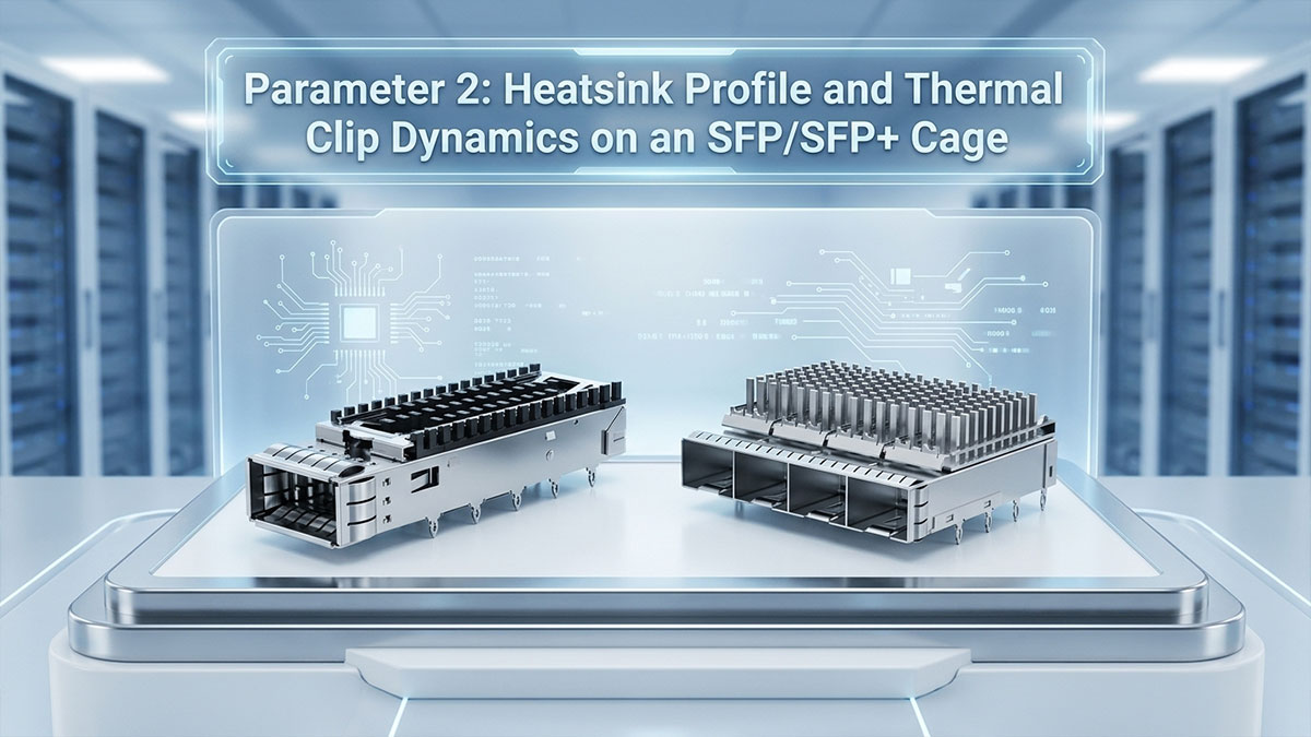
🔷 Parameter 2: Kühlkörperprofil und Dynamik der thermischen Klammern an einem SFP/SFP+-Käfig
Sobald der Käfig mechanisch auf der Platine befestigt ist, wird die Wärmeableitung zum nächsten Hauptfaktor für die Systemzuverlässigkeit. SFP+-Transceiver verbrauchen typischerweise mehr Leistung als herkömmliche Gigabit-Module und benötigen daher direkte Wärmeableitungsmechanismen oberhalb des Metallgehäuses. Die Abstimmung von Kühlkörpergeometrie, Luftstromgeschwindigkeit und Anpressdruck der mechanischen Klemmen ist entscheidend, um die Betriebstemperatur der Hochgeschwindigkeitsoptiken innerhalb ihrer zulässigen Grenzwerte zu halten.
Optionen für die Kühlkörperhöhe und Grenzen der Gehäusefreiheit
Die Höhe des Kühlkörpers bestimmt direkt die verfügbare Wärmeabfuhrfläche, ist aber durch den vertikalen Abstand von 1U- oder Mehrsteckplatz-Rackgehäusen begrenzt. Standardhöhen – am häufigsten 4.2 mm, 6.5 mm und 13.5 mm – eignen sich für unterschiedliche Leistungsanforderungen und mechanische Umgebungen.
Die nachstehende Auswahlmatrix zeigt gängige Profilgrenzen auf:
| Profilhöhe | Typische Anwendung | Vertikale Durchfahrtshöhe | Primäre Luftstrombegrenzung |
| 4.2 mm (niedriges Profil) | Extrem kompakte 1U-Blade-Server und PCIe-Karten | Geringer Platz nach oben (< 6 mm über dem Käfig) | Benötigt Lüfter mit hohem statischen Druck. |
| 6.5 mm (Standard) | Allgemeine 1U-Unternehmensschalter | Mäßige Kopffreiheit (8-10 mm über dem Käfig) | Ausgeglichener Luftstromwiderstand |
| 13.5 mm (Hoch/Verlängert) | Offenes 2U+-Gehäuse & Hochleistungsoptik | Ausreichend Freiraum (> 15 mm über dem Käfig) | Hocheffiziente natürliche/erzwungene Konvektion |
Die Wahl eines zu hohen Kühlkörpers birgt das Risiko direkter Interferenzen mit den Gehäusedeckeln oder benachbarten Mezzanine-Karten. Umgekehrt kann ein zu niedriges Profil bei kontinuierlicher 10G-Übertragung zu einer Drosselung der optischen Leistung führen.
Luftwiderstand bei Stiftrippen vs. geraden Rippen
Die Geometrie der Kühlrippen bestimmt, wie effizient die erzwungene Konvektion die Wärme von einem SFP+-Gehäuse abführt. Gerade Kühlrippen leiten die Luft parallel zur Länge des Transceivers und bieten so einen geringen Luftwiderstand, erfordern jedoch eine streng unidirektionale Luftströmung. Stiftrippen erzeugen gezielt Mikroturbulenzen und verbessern dadurch die multidirektionale Wärmeabfuhr in komplexen Lüfterkanalanordnungen.
Die Auswahl des passenden Lüfters erfordert den Abgleich der Luftvolumenstrom-Werte (CFM) der Gehäuselüfter mit den Widerstandskurven der Lamellen. Falsch ausgerichtete, gerade Lamellen können dazu führen, dass interne optische Laser nicht ausreichend gekühlt werden, wenn Luft durch Öffnungen mit dem geringsten Widerstand entweicht.
Gleichgewicht zwischen Haltekraft der Klammer und Kontaktdruck
Die Thermoklammer erzeugt die notwendige, kontinuierliche Normalkraft, um den Kühlkörper an der Oberseite des SFP/SFP+-Käfigs zu fixieren. Ist die Klammer zu schwach, entstehen Luftspalte und der Wärmewiderstand steigt sprunghaft an. Ist sie hingegen zu steif, kann der zu hohe Druck die obere Blechabdeckung verformen und die internen Führungsschienen des Moduls einklemmen.
Wichtige Faustregel: Die Modulschnittstelle sollte einen dauerhaften Kontaktdruck von 10 bis 15 psi (ca. 70 bis 100 kPa) aufweisen. Bei einer Standard-SFP-Gehäuseoberseite (ca. 15 mm x 10 mm) entspricht dies einer Normalkraft von etwa 10 bis 15 N. Dieser Wert gewährleistet einen optimalen thermischen Kontakt ohne Blockieren des Transceivers oder mechanische Verriegelung.
Die mechanische Ermüdung von gestanzten Federstahlklammern muss über die gesamte Lebensdauer des Systems berücksichtigt werden. Längere Temperaturwechsel können die Klammerspannung verringern und so die Wärmeübertragungsleistung im Laufe der Jahre im Feldeinsatz allmählich verschlechtern.
Kompressionsverhalten von Wärmeleitmaterialien (TIM)
Für eine effektive Wärmeübertragung müssen die mikroskopisch kleinen Luftspalte zwischen dem rauen Metallgehäuse und der Unterseite des Kühlkörpers gefüllt werden. Phasenwechselmaterialien und auflösbare Spaltpads werden häufig eingesetzt, um den thermischen Widerstand an der Grenzfläche zu verringern, ihre Wirksamkeit hängt jedoch stark von der mechanischen Kompressionsrate ab.
Wichtige mechanische Aspekte bei Wärmeleitpasten sind:
- Optimales Kompressionsverhältnis: Die Kontaktflächen sollten auf 30 bis 50 % ihrer Nenndicke komprimiert werden, um den Kontaktwiderstand zu minimieren, ohne die Leiterbahnen auf der Platine zu überlasten.
- Oberflächenbenetzung & Kriechen: Sicherstellen, dass die thermischen Phasenwechselmaterialien unter dynamischen thermischen Belastungen eingeschlossen bleiben, um ein Eindringen von Silikon in nahegelegene optische Bohrungen zu verhindern.
- Toleranz gegenüber Dickenabweichungen: Ein Budget für anfängliche Abweichungen der TIM-Dicke (typischerweise ±10%) innerhalb des gesamten Toleranzbereichs der Käfigklammer, um eine gleichbleibende Kontaktkraft zu gewährleisten.
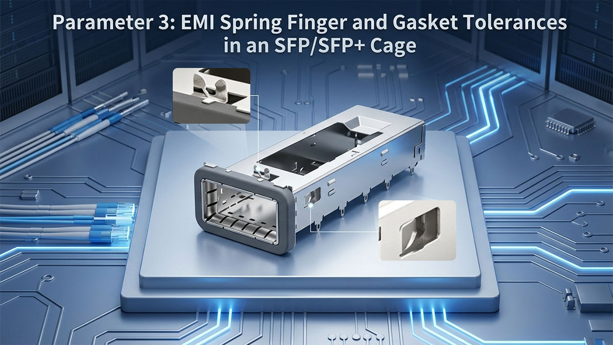
🔷 Parameter 3: Toleranzen für EMI-Federfinger und Dichtung in einem SFP/SFP+-Käfig
Effiziente Wärmeleitwege sorgen zwar für die interne Kühlung der Hochleistungsoptik, doch die hohen Übertragungsgeschwindigkeiten von 10G-Signalen führen zwangsläufig zu erhöhter elektromagnetischer Interferenz (EMI) an der Gehäusegrenze. Die Schnittstelle zwischen Gehäusevorderseite und Frontblende dient als primärer Schutz gegen HF-Abstrahlung in benachbarte Geräte. Die Verwendung von elastischen Federkontakten oder leitfähigen Elastomerdichtungen gewährleistet eine kontinuierliche Erdung, ohne das Modul bei einem Hot-Swap im laufenden Betrieb zu blockieren.
Kontaktfedermaterialien: Berylliumkupfer vs. Edelstahl
Die Wahl des Federfingermaterials bestimmt die mechanische Elastizität, die Dauerfestigkeit und die elektrische Langzeitleitfähigkeit eines SFP- oder SFP+-Käfigs. Berylliumkupfer (CuBe) bietet eine überlegene Leitfähigkeit und Elastizität unter dynamischer Biegung, während Edelstahl eine höhere mechanische Streckgrenze bei geringeren Herstellungskosten ermöglicht.
Eine vergleichende Bewertung verdeutlicht die physikalischen Vor- und Nachteile dieser gängigen Legierungsoptionen:
| Materialattribut | Berylliumkupfer (CuBe) | Edelstahl (SUS 301/304) |
| Elektrische Leitfähigkeit | Hoch (20 % bis 28 % IACS) | Niedrig (2 % bis 3 % IACS) |
| Elastizitätsbereich und Spannungsrelaxation | Großer Elastizitätsbereich; minimale Entspannung im Laufe der Zeit | Engeres elastisches Fenster; neigt zur Relaxation bei anhaltender Auslenkung |
| Beschichtungshaftung | Hervorragend geeignet für helle Zinn- oder Nickeloberflächen | Erfordert spezielle Passivierungs-/Sperrschichtbeschichtung |
| Korrosionsbeständigkeit | Mäßig (stark abhängig von der Beschichtungsschicht) | Hohe von Natur aus hohe Beständigkeit gegen Oxidation |
| Kosten | Höhere Rohstoff- und Wärmebehandlungskosten | Wirtschaftliche Wahl für kostensensible Schalter |
Kompressionshubbegrenzungen und Blendenabstand
Um einen gleichmäßigen Kontakt über den gesamten Umfang der Aussparung in der Lünette zu gewährleisten, ist eine präzise Steuerung des Federwegs erforderlich. Ist der Arbeitsweg zu gering, können Fertigungstoleranzen im Gehäuseblech zu intermittierenden Luftspalten führen, durch die HF-Energie austreten kann. Umgekehrt führt eine Überdehnung der Federlaschen über ihre Elastizitätsgrenze hinaus zu bleibenden Verformungen und dem Abscheren der Kontaktfinger.
Die mechanischen Grenzen für den Standard-Lünetteneingriff folgen im Allgemeinen diesen Maßregeln:
- Nominaler Arbeitshub: Ziel ist ein Kompressionsdurchbiegungsbereich zwischen 1.0 mm und 1.5 mm bei vollständig sitzender Frontplatte.
- Randfreier Spalt: Zwischen der äußeren Käfigwand und der Rohkante des Lünettenausschnitts muss ein nominaler Luftspalt von 0.3 mm bis 0.5 mm eingehalten werden.
- Vorspannungs-Ablenkwinkel: Geben Sie einen Fingereintrittswinkel von 15° bis 20° an, um ein reibungsloses Einschieben ohne Blockieren oder Knicken zu gewährleisten.
- Elastische Sicherheitsmarge: Es muss sichergestellt werden, dass die Fingergeometrie mindestens 130 % des maximal zu erwartenden Hubs aushält, ohne die Streckgrenze des Materials zu überschreiten.
Stabilität des Kontaktwiderstands über Steckzyklen hinweg
Bei wiederholten Hot-Swap-Zyklen kann die mechanische Reibung die Schutzkontaktbeschichtung abtragen und zu schnellem Reibverschleiß führen. Eine ideale SFP/SFP+-Käfigschnittstelle gewährleistet eine stabile elektrische Kontinuität, indem der Massekontaktwiderstand über die gesamte Lebensdauer des Systems unter 50 mΩ gehalten wird.
Umwelteinflüsse wie Luftfeuchtigkeit und Sulfide in der Luft können unbeschichtete Grundmetalle an mikroskopischen Kontaktstellen oxidieren. Durch die Verwendung von Opferzinn oder selektiver Goldbeschichtung auf der Kontaktfläche wird galvanische Korrosion verhindert. Für vergoldete Kontaktflächen sollte eine Mindestdicke von 0.76 µm (30 µin) angegeben werden, um mehr als 250 Steckzyklen standzuhalten, ohne die darunterliegende Nickelbarriereschicht freizulegen. Dies gewährleistet, dass die Masseverbindungen auch nach Hunderten von Modulsteckvorgängen leitfähig bleiben.
Abwägung zwischen Einfügungskraft und Abschirmwirkung
Um eine effektive Abschirmung gegen 10-GHz-Oberwellen zu gewährleisten, ist eine hohe Kontaktkraft erforderlich, um hochfrequente Resonanzen zu eliminieren. Eine Erhöhung der Federraten der einzelnen Finger vervielfacht jedoch die gesamte Einsteckkraft, die zum Einsetzen eines SFP-Käfigs in ein Multiport-Gehäuse benötigt wird, was die werkzeuglose Wartung für Endbenutzer erschwert.
Ingenieure müssen ein optimales Betriebsfenster festlegen, das sowohl den Vorschriften als auch den ergonomischen Anforderungen gerecht wird:
- Das EMI-Ergonomiefenster: Eine Normalkraft von 0.3 N bis 0.6 N pro Finger wird angestrebt. Dies gewährleistet eine zuverlässige Hochfrequenz-HF-Dämpfung (> 40 dB bei 10 GHz) und begrenzt gleichzeitig die gesamte Einsteckkraft eines Einzelport-Käfigs auf unter 18 N (ca. 4 lbf) für ein müheloses Hot-Plugging von Modulen.
Diese maximale Einsteckkraft von 18 N berücksichtigt die kombinierte Wirkung der Reibung der EMI-Feder, des Widerstands der internen Führungsschiene und der Vorspannung der Transceiver-Verriegelung. Bei einer typischen 6-Finger-Blende mit einem Reibungskoeffizienten von 0.4 beträgt der Beitrag der EMI-Feder allein etwa 6 × 0.45 N × 0.4 ≈ 1.1 N. Der verbleibende Spielraum berücksichtigt den mechanischen Widerstand und das Einrasten der Verriegelung.
Wird dieses Kräfteverhältnis nicht ausgeglichen, entsteht übermäßige Reibung, die die Oberflächen der Frontplatte zerkratzt oder das vollständige Einrasten der Modulverriegelungen verhindert. Durch die Feinabstimmung des Federabstands und der Profilgeometrie können Entwickler die Anforderungen an die elektromagnetische Verträglichkeit (EMV) mit der mechanischen Nutzbarkeit in Einklang bringen – ein entscheidender Kompromiss im Auswahlprozess.
🔷 Parameter 4: Lichtleiterstruktur und optische Ausrichtung für einen SFP/SFP+-Käfig
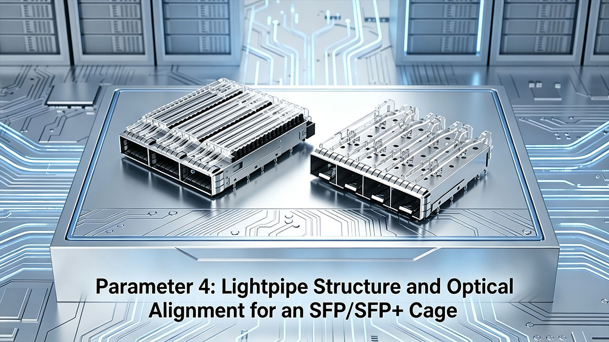
Neben der Gewährleistung mechanischer Integrität und thermischer Stabilität benötigt Netzwerkhardware eine klare visuelle Telemetrie für Portstatus und Datenaktivität. Die Integration transparenter Polycarbonat-Lichtleiter direkt in die Gehäusekonstruktion leitet Licht von auf der Platine montierten LEDs zur Frontplatte, ohne dass zusätzliche Verkabelung erforderlich ist. Für eine optimale optische Ausgabe ist jedoch eine präzise physische Ausrichtung zwischen dem Lichtleitereinlass und dem darunterliegenden Leiterplattenlayout unerlässlich, da die Toleranzen der mechanischen Ausrichtung die Effizienz der optischen Kopplung direkt beeinflussen.
Einzel- vs. Zweikanal-Lichtleiterkonfigurationen
Einkanalige Lichtleiter unterstützen die grundlegende Verbindungserkennung, während Zweikanalkonfigurationen separate Anzeigen für Verbindungsgeschwindigkeit und Datenverkehrsaktivität pro Port bereitstellen. Zweikanalige Designs erfordern interne optische Trennwände oder dedizierte physische Luftspalte, um Lichtstreuung zwischen benachbarten Anzeigekanälen zu verhindern.
Die Wahl zwischen den beiden Varianten bestimmt die physische Komplexität des oberen Gehäuses eines SFP/SFP+-Käfigs. Bei Mehrkanal-Implementierungen muss ein Gleichgewicht zwischen engen Toleranzen beim Kunststoffspritzguss und ausreichender mechanischer Steifigkeit gefunden werden, um Verformungen beim Einsetzen der Module zu vermeiden.
Äußere, innere und obere Lünettenausgänge
Der Austrittspunkt des Lichtleiters an der Frontplatte bestimmt die Lesbarkeit des Panels und den Platzbedarf für die interne Kabelführung. Bei seitlichem Lichtaustritt nach außen verläuft das Licht entlang der Außenwände eines SFP/SFP+-Käfigs und ist somit von den Panelkanten aus sichtbar. Bei seitlichem Lichtaustritt nach innen befindet sich der Lichtleiter zwischen benachbarten Ports, wodurch Platz im Rahmen für hochdichte 1×N-Layouts gespart wird. Beide Geometrien eignen sich am besten für einreihige Layouts mit offenem horizontalem Abstand.
Bei Konfigurationen mit Top-Exit wird das Licht direkt über die obere Abdeckung eines SFP+-Käfigs geleitet, wodurch horizontaler Platz auf der Platine für eine engere Anordnung mehrerer Ports erhalten bleibt. Allerdings muss die Lichtführung von oben sorgfältig mit den Kühlkörperklammern abgestimmt werden, um physische Interferenzen zwischen der optischen Leitung und der Kühllösung zu vermeiden.
Innerer Biegeradius und optische Übertragungsdämpfung
Die Lichtdurchlässigkeit durch transparenten optischen Kunststoff beruht ausschließlich auf Totalreflexion entlang gekrümmter Lichtleiter. Ist der innere Krümmungsradius kleiner als das Doppelte der Kerndicke (R < 2D), tritt Licht durch die äußere Mantelkrümmung aus und reduziert die Helligkeit der Anzeige auf der Frontblende erheblich.
Optische Verluste summieren sich in tiefen Käfigkonstruktionen über lange Kabelwege rapide. Die Verwendung von geformten optischen Stufen oder polierten 45°-Innenspiegeln minimiert die Dämpfung und sorgt für eine gleichmäßige Ausleuchtung der Frontplatte, ohne die LEDs auf der Platine zu übersteuern.
Oberflächenmontierbare LED-Grundfläche und optische Zielvorrichtung
Der Lichteintrittsfuß des Lichtleiters muss exakt mittig über der Emissionsfläche der SMD-LED auf der Leiterplatte positioniert sein. Selbst eine seitliche Abweichung von ±0.3 mm – deutlich innerhalb der üblichen Fertigungstoleranzen bei Leiterplatten – kann die Lichtauskopplungseffizienz um bis zu 40 % reduzieren und zu schwachen oder ungleichmäßigen Displayanzeigen führen.
Die Ingenieure müssen zudem einen vertikalen Luftspalt von 0.2 mm bis 0.4 mm zwischen der LED-Linse und der Lichtleitereinlassfläche einhalten. Dieser Abstand gleicht die Flexibilität der Leiterplatte während der Presspassung des Gehäuses aus und verhindert strukturelle Beschädigungen der empfindlichen, verlöteten LED-Gehäuse.
🔷 Parameter 5: Toleranzen für gestapelte und gruppierte Dichte in einem SFP/SFP+-Käfig
Die Skalierung von Single-Port-Architekturen zu hochdichten Multiport-Switches vervielfacht die mechanischen Anforderungen. Zwar erhöhen gestapelte (1xN) und gebündelte (2xN) Konfigurationen die Anzahl der Ports auf der Vorderseite drastisch, konzentrieren aber gleichzeitig Einfügungsspannungen und Wärmeableitung auf engstem Raum. Die Kontrolle der Innenwandabmessungen, der vertikalen Ausrichtung und der Koplanarität der Komponenten in Multiport-Baugruppen ist daher unerlässlich, um die strukturelle Integrität zu gewährleisten und Signalverluste zu vermeiden.

Teilung und Wandstärke von einreihigen, verketteten Käfigen
Bei gruppierten Multiport-Gehäusen (z. B. 1x2, 1x4 oder 1x6) bestimmt der Abstand zwischen den Ports sowohl den horizontalen Abstand der Frontplatte als auch die zulässige Dicke der internen Trennwände. Der branchenübliche Abstand beträgt typischerweise 14.25 mm (Mitte zu Mitte), wodurch extrem dünne Metalltrennwände zwischen benachbarten Modulen entstehen.
| Designparameter | Standardabmessung | Auswirkungen auf die Technik und Toleranzrisiko |
| Port-zu-Port-Pitch | 14.25 mm nominal | Eine kumulative Rasterabweichung innerhalb eines 1x6-Käfigs kann zu einer Blockierung der Gehäuseblende führen. |
| Innenwandstärke | 0.20mm zu 0.25mm | Dünnere Wände verringern zwar den Abstand zwischen den Anschlüssen, erhöhen aber das Risiko von strukturellem Ausknicken. |
Sind die Trennwände im Inneren aus Platzgründen zu dünn, kann das Einsetzen eines SFP-Käfigmoduls benachbarte Steckplätze verformen und so benachbarte Transceiver stören. Entwickler müssen daher eine hohe Portdichte mit ausreichender struktureller Verstärkung zur Aufnahme seitlicher Einsteckkräfte in Einklang bringen. Neben der mechanischen Integrität müssen dünne Trennwände auch durchgehende Masseverbindungen gewährleisten, um die für die EMV-Konformität von Mehrkanalsystemen erforderliche Port-Isolation von >40 dB bei 10 GHz zu erreichen.
Vertikale Durchfahrtshöhe für zweireihige, gestapelte Käfige (2xN)
Gestapelte Architekturen (2x1, 2x4, 2x8) verdoppeln die Portdichte, indem obere und untere Transceiver-Ports in einem gemeinsamen Gehäuse untergebracht werden. Da der obere Port bis zu 25 mm über der Leiterplattenoberfläche liegt, erzeugen die Einsteckkräfte eine erhebliche mechanische Hebelwirkung und ein Drehmoment auf die darunterliegenden Löt- oder Presspassungsstifte.
Um eine zuverlässige Verbindung zwischen den beiden Ebenen zu gewährleisten, müssen die vertikalen mechanischen Abstände strengen baulichen Vorgaben entsprechen:
- Abstand zwischen den Modulschächten: Zwischen den oberen und unteren Modulfeldern muss eine Zwischenblechplatte von mindestens 1.5 mm Dicke vorhanden sein, um Erdungsanschlüsse und Lichtleiterleitungen aufzunehmen.
- Vertikales Einschubmoment: Stellen Sie sicher, dass die Verankerungsbolzen an der Basis beim Einsetzen der Module in die obere Ebene eine nach unten gerichtete Drehkraft von bis zu 35 N aufnehmen können.
- Ausrichtung der Aussparungen in der Lünette: Die vertikale Achsenabweichung der Anschlüsse darf bei allen Anschlüssen nicht über ±0.15 mm hinausgehen, um zu verhindern, dass die Verriegelungen des Transceivers an der Frontplatte hängen bleiben.
Toleranzen für die Koplanarität integrierter Steckverbinder
Im Gegensatz zu Single-Port-Designs mit separaten Kartenrandbuchsen verfügen gestapelte Multi-Port-SFP+-Käfigbaugruppen über integrierte, zweistufige interne Steckverbinder. Diese Mehrpolbaugruppen zeichnen sich durch verlängerte interne Leadframes aus, die von den oberen Portkontakten zu den Lötpads der Host-Leiterplatte verlaufen.
- Kritische Grenze für die Koplanarität: Die Koplanarität der Leadframe-Pins muss innerhalb eines strengen Bereichs von 0.10 mm über die gesamte Multiport-Anordnung hinweg gewährleistet sein.
Abweichungen über diesem Schwellenwert hinaus führen dazu, dass nicht-koplanare Pins beim Reflow-Löten über den Lötpastenablagerungen schweben und dadurch zeitweise Unterbrechungen an Hochgeschwindigkeits-Differenzialpaaren verursachen. Bei Presspassvarianten bewirken ungleichmäßige Pinhöhen ein versetztes Einstecken, wodurch die mechanische Kraft auf einzelne Pins konzentriert wird und die durchkontaktierten Lötösen der Leiterplatte brechen können.
Kontrolle von thermischer Spannung und Leiterplattenverzug
Dicht gepackte Multiport-Arrays konzentrieren die Wärmeabfuhr mehrerer aktiver Transceiver auf wenige Bereiche der Leiterplatte und erzeugen so starke Temperaturgradienten. Beim Reflow-Löten und bei hoher Datenübertragungsrate führen unterschiedliche Wärmeausdehnungskoeffizienten (CTE) zwischen dem starren Metallkäfig und dem organischen Leiterplattenlaminat zu lokalen Verformungen der Leiterplatte.
Um Verformungen bei großen, gestapelten Baugruppen zu minimieren, sind sorgfältige Konstruktions- und Fertigungssicherheitsvorkehrungen erforderlich:
- Ausgewogenes Masseanschlussmuster: Die eingepressten Masseanschlüsse sind symmetrisch über die Käfiggrenze verteilt, um eine lokale mechanische Zugbelastung während der thermischen Ausdehnungszyklen zu verhindern.
- PCB-Versteifungsstreben: Mechanische Versteifungswinkel oder Trägerplatten werden auf Rückwandplatinen integriert, die 2x6 oder größere Multiport-SFP/SFP+-Käfig-Arrays unterstützen.
- Thermische Entlastungsabstände: Optimieren Sie die Geometrie der thermischen Entlastung des Kupfers um die hochdichten Pin-Pads, um eine gleichmäßige Wärmeverteilung während des Reflow-Lötens bei der Montage zu gewährleisten.
🔷 Wie führt man eine Analyse der mechanischen Toleranzen für einen SFP/SFP+-Käfig durch?
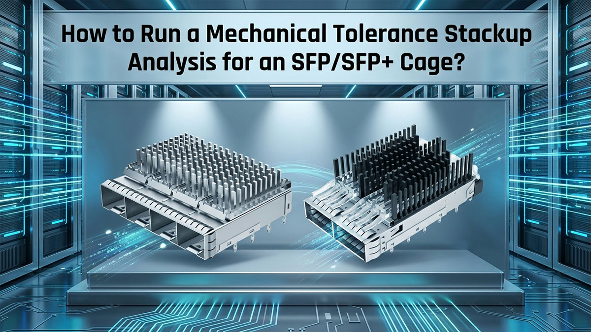
Die isolierte Bewertung einzelner Parameter liefert wertvolle Basisdaten, doch die Zuverlässigkeit im realen Einsatz hängt davon ab, wie diese Dimensionen im Zusammenspiel miteinander interagieren. Eine umfassende Toleranzanalyse fasst Fertigungs-, Montage- und Gehäuseabweichungen in einem einzigen prädiktiven mechanischen Modell zusammen. Die frühzeitige Durchführung dieser Berechnung verhindert kostspielige Nachbesserungen am Gehäuseblech und gewährleistet eine gleichbleibende Transceiver-Passung über alle Produktionschargen hinweg.
Berechnung der kumulativen Dimensionsabweichungen im ungünstigsten Fall
Die Toleranzanalyse kombiniert im Allgemeinen die Worst-Case-Analyse (WCA) mit der statistischen Modellierung der Wurzel der Quadratsumme (RSS). Die WCA geht davon aus, dass sich alle physikalischen Abmessungen gleichzeitig auf ihre extremen Grenzwerte verschieben und definiert so den absoluten Worst-Case-Bereich, um ein Blockieren zu verhindern. Im Gegensatz dazu behandelt die RSS-Modellierung Fertigungstoleranzen als Standardverteilungen und bietet so ein realistisches und kosteneffizientes Gleichgewicht zwischen Montageausbeute und Ausschussquote.
Zu den wichtigsten Maßfaktoren entlang der horizontalen und vertikalen Montageschleifen gehören:
| Dimensionsvariable in der Schleife | Nennmaß | Typischer Toleranzbereich | Modellierungsauswirkungen |
| Breite des Gehäuserahmenausschnitts | 14.80 mm | ± 0.10mm | Beeinflusst direkt die seitlichen Kompressionsgrenzen der Federfinger |
| Breite des äußeren Käfigumschlags | 14.00 mm | ± 0.08mm | Legt den nominalen Luftabstand zum Lünettenrahmen fest. |
| Leiterplattenrand-zu-Käfig-Pinposition | 0.00 mm (Bezugspunkt) | ± 0.05mm | Führt eine seitliche Schräglage ein und verschiebt den Käfig relativ zur Lünettenöffnung. |
| Höhe der Motherboard-Abstandshalter | 6.00 mm | ± 0.08mm | Verschiebt die vertikale Portausrichtung relativ zur Frontplatte |
Wenn das kumulative Spiel unter ungünstigsten Bedingungen gegen null tendiert, klemmen die optischen Module bei der Installation am Rahmenrand an. Mithilfe von RSS-Modellierung und Fertigungstoleranzen von ±3σ sollten Hardware-Teams eine statistische Spielreserve von mindestens 0.25 mm anstreben, um unvorhergesehene Fertigungsabweichungen auszugleichen.
Bei Konstruktionen mit hohen Kühlkörperprofilen (13.5 mm oder höher) müssen die vertikalen Komponenten – einschließlich Abstandshalterhöhe und Leiterplattenverzug – gemeinsam analysiert werden, um ausreichend Platz für den Deckel zu gewährleisten. Für solche Fälle wird eine separate Analyse der vertikalen Schleife empfohlen.
Abstandsregeln für Platinenkanten und Frontplatten
Die präzise räumliche Positionierung zwischen der Vorderkante der Platine und der inneren Frontplattenbegrenzung ist entscheidend für das korrekte Einrasten der Verriegelungen. Sitzt der SFP-Käfig zu weit hinter der Frontplatte, können die Transceiver-Halteklammern nicht sicher in den Aussparungen des Käfigs einrasten. Ist er zu weit vorne montiert, stößt die Käfigspitze an die innere Blechoberfläche, wodurch die Leiterplatte nicht bündig an den Gehäusebefestigungspunkten anliegt.
Planer sollten klare Abgrenzungsregeln befolgen, um die erforderlichen physischen Abstände einzuhalten:
- Abstand zur Platinenkante: Zwischen der Vorderkante der Leiterplatte und dem inneren Gehäuseflansch muss ein Mindestabstand von 1.25 mm ± 0.15 mm eingehalten werden.
- Durchdringung des Verriegelungsfensters: Stellen Sie sicher, dass die Verriegelungslaschen des Moduls mindestens 0.8 mm durch die Verriegelungsöffnung des Käfigs hindurchdringen, um ein versehentliches Trennen unter Kabelspannung zu verhindern.
- Kompressionsfenster der Lünettendichtung: Prüfen Sie, ob die gesamte axiale Bewegungsfreiheit die peripheren EMI-Federfinger nicht über ihre maximale elastische Streckgrenze von 70 % hinaus komprimiert.
Werkzeugvorrichtungen und automatisierte Bestückungsmargen
Hochgeschwindigkeits-SMD-Bestückungsanlagen benötigen spezielle Freiräume für die Handhabung und Montage schwerer Mehrkanalgehäuse. Greifdüsen und mechanische Presspassungsköpfe benötigen definierte Sperrzonen, die frei von einzelnen Kondensatoren, Widerständen und Messpunkten sind.
Werkzeug-Sperrabstand: Um den gesamten Umfang des SFP+-Käfigs herum ist ein Mindestabstand von 3.0 mm einzuhalten, der sich auf 5.0 mm an der hinteren Stiftleiste erweitert, um Platz für die automatisierten Presspasswerkzeuge zu schaffen. Bei Presspass-Käfigvarianten muss die Parallelität der oberen Auflageplatte der Montagevorrichtung – typischerweise ±0.05 mm – anhand der in Parameter 5 für Mehrfachsteckverbinder festgelegten Koplanaritätstoleranz überprüft werden. Eine zu starke Neigung der Auflageplatte kann das Stifthöhenprofil des Käfigs über den Grenzwert von 0.10 mm hinaus verschieben, selbst wenn alle Komponententoleranzen einzeln eingehalten werden.
Darüber hinaus müssen die Vakuumbereiche der dynamischen Bestückungsdüsen mit dem Schwerpunkt des Gehäuses übereinstimmen. Asymmetrische, oben angebrachte Kühlkörperklammern können zu Rotationsabweichungen bei der Bestückung führen, was Pin-Fehlausrichtungen und verbogene Anschlüsse während der automatisierten Hochgeschwindigkeits-Leiterplattenbestückung zur Folge haben kann.
🔷 Fazit: Wichtigste Erkenntnisse zur Auswahl des richtigen SFP/SFP+-Käfigs
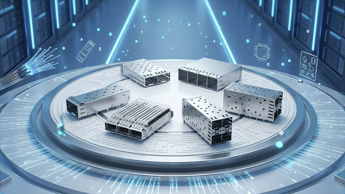
Standard-MSA-Spezifikationen liefern zwar die grundlegenden Abmessungen, die tatsächliche Zuverlässigkeit hängt jedoch von der Einhaltung mechanischer Toleranzen jenseits der Standardzeichnungen ab. Für einen reibungslosen Betrieb im Feld müssen Anschlussmethoden, Wärmeableitung und Schirmungsfestigkeit an die realen Betriebsbedingungen Ihrer Hardware angepasst werden. Durch die frühzeitige Berücksichtigung mechanischer Parameter in der Leiterplattenentwicklungsphase können Entwicklungsteams Montagefehler vermeiden, Signalstörungen reduzieren und Ausfälle der Verriegelung im Feld verhindern.
Praktische Strategie zur Auswahl von Ingenieuren
Bei der Bewertung von Kandidaten für Single-Port-SFP-Käfige oder dichte Multi-Port-SFP+-Käfige sollten strukturelle Belastbarkeit und thermische Anforderungen Vorrang vor den reinen Stückkosten haben. Eine systematische Validierung muss die Fertigungsmöglichkeiten mit den kontinuierlichen Betriebsbelastungen im Gehäuse in Einklang bringen.
Nutzen Sie diese gezielte Checkliste, um Ihre Konstruktion anhand der fünf oben genannten mechanischen Parameter zu validieren:
Montageverfahren: Für Systeme mit starken Vibrationen und häufigem Einstecken eignen sich nachgiebige Presspassstifte; für kostensensible Designs mit geringerer Einsteckfrequenz empfiehlt sich SMT- oder PIP-Löten.
- Thermische Anpassung: Die Verlustleistung des Transceivers sollte mit geeigneten Kühlkörperhöhen (4.2 mm/6.5 mm/13.5 mm) abgestimmt werden, die Lamellengeometrie sollte an den Luftstrom im Gehäuse angepasst werden und eine Klemmkraft von 10-15 psi (10-15 N) bei einer Wärmeleitpastenkompression von 30-50 % angestrebt werden.
- EMV-Dichtungen: Für Anwendungen mit hoher Zyklusbelastung wählen Sie Berylliumkupferfedern mit einer Goldbeschichtung von ≥ 0.76 µm. Bei kostensensiblen Anwendungen kann passivierter Edelstahl ausreichend sein. Die angestrebte Normalkraft beträgt 0.3–0.6 N pro Finger. Stellen Sie sicher, dass der Kompressionshub von 1.0–1.5 mm innerhalb der elastischen Sicherheitsmarge von 130 % bleibt.
- Optische Ausrichtung: Zentrieren Sie den Lichtleitereinlass über der emittierenden Fläche der LED (±0.3 mm Kopplungsverlustschwelle) und halten Sie einen vertikalen Abstand von 0.2-0.4 mm ein, um eine Beschädigung des LED-Gehäuses zu vermeiden.
- Toleranzen bei gestapelten Gehäusen: Eine Koplanaritätsgrenze von 0.10 mm für den Leadframe ist einzuhalten, und ein Mindestabstand von 1.5 mm zwischen den Gehäuseunterseiten ist bei 2×N gestapelten Gehäusen zu gewährleisten.
- Werkzeugspielraum: Um jeden SFP/SFP+-Käfig herum muss ein Sicherheitsabstand von 3.0 mm eingehalten werden (5.0 mm auf der hinteren Stiftleiste), um ausreichend Platz für die automatische Bestückung und Montage sowie für Presspassungswerkzeuge zu gewährleisten.
Die Durchführung einer vollständigen statistischen Toleranzanalyse – unter Verwendung sowohl der WCA- als auch der RSS-Methode – vor dem endgültigen Festlegen des Leiterplattendesigns gewährleistet hohe Fertigungsausbeuten und einen zuverlässigen Moduleingriff.
Sobald die Toleranzanalyse abgeschlossen und die mechanischen Anforderungen definiert sind, besteht der nächste Schritt darin, einen Lieferanten zu finden, der Gehäuse liefern kann, die diesen Spezifikationen entsprechen. Die Zusammenarbeit mit einem Anbieter, der sowohl MSA-konforme als auch kundenspezifische Verbindungslösungen anbietet, vereinfacht den Übergang von der Designvalidierung zur Produktion.
Entdecken Sie das umfangreiche Portfolio an SFP/SFP+-Gehäusen und Netzwerkverbindungen bei LINK-PP Offizieller Shop um die ideale Lösung für Ihr nächstes Hochgeschwindigkeitsdesign zu finden.