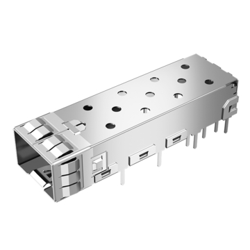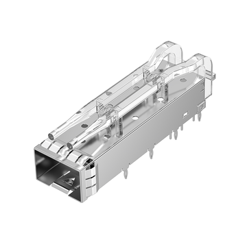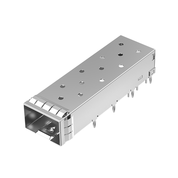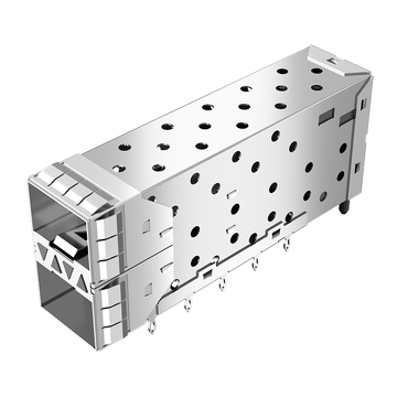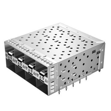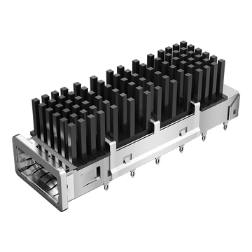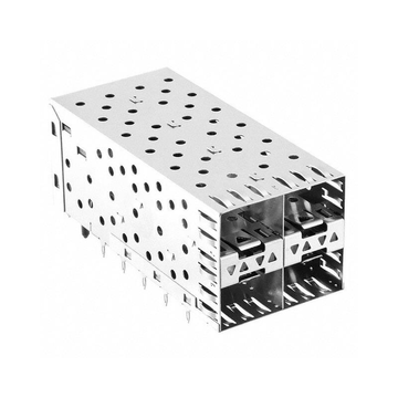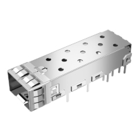
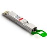
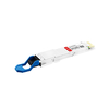
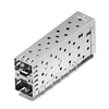
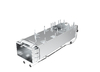
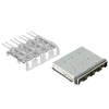

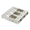

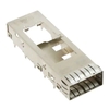
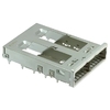
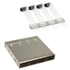
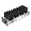


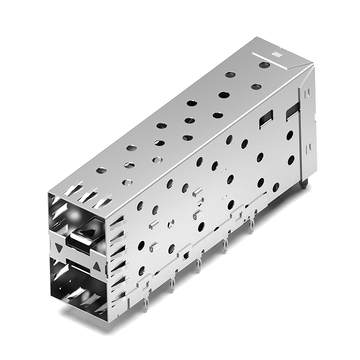



SFP cage assembly is a critical step in networking hardware manufacturing. Although the cage may appear to be a simple metal enclosure for optical transceivers, its installation directly affects PCB integrity, mechanical alignment, EMI shielding, and front-panel integration. Even small assembly deviations can lead to repeated rework, functional failures, and reduced first-pass yield.
Many SFP cage assembly defects originate from incorrect stencil design, poor LED positioning, uncontrolled press-fit insertion, or dimensional mismatches between the PCB and chassis. These problems are particularly challenging because some defects remain hidden until functional testing, module insertion, or EMC verification.
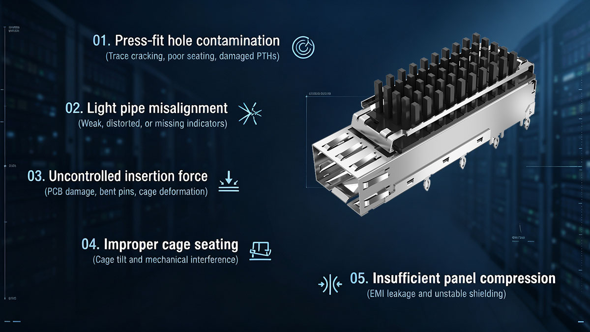
This guide examines five common SFP cage assembly defects and explains how to identify their root causes and prevent production failures:
-
Solder paste contamination in press-fit holes.
-
Light pipe and SMD LED misalignment.
-
Uncontrolled press-fit insertion force.
-
Improper cage seating and PCB coplanarity.
-
Insufficient front-panel compression and EMI contact.
It also provides practical DFM checks, inspection methods, and component selection considerations to help engineering and manufacturing teams improve PCB assembly consistency.
Why SFP Cage Assembly Defects Have a Direct Impact on PCB Yield
SFP cage assembly defects can affect more than the physical installation of a metal enclosure. They can compromise PCB mounting holes, optical indicators, grounding paths, and mechanical interfaces, resulting in both immediate production failures and latent reliability problems.
Understanding how the cage interacts with the PCB, transceiver, and front panel is the first step toward preventing these defects.
The Role of an SFP Cage in PCB-Level Integration
An SFP cage is a metal enclosure that houses and mechanically supports an SFP optical transceiver or compatible copper module. It also provides EMI shielding and, depending on the design, thermal management and optical status indication.
A typical SFP cage assembly performs several functions:
-
Mechanical retention: Holds the transceiver in position and guides insertion and extraction.
-
EMI shielding: Creates a conductive enclosure around the transceiver to limit electromagnetic interference.
-
PCB integration: Uses press-fit compliant pins or other mounting structures to secure the cage to the host board.
-
Thermal management: Provides ventilation openings or integrates a heatsink to support heat dissipation.
-
Optical indication: Uses an optional light pipe to transmit LED status signals toward the front panel.
The specific configuration depends on the cage design. For example, some assemblies use compliant press-fit tails and external EMI spring fingers, while others incorporate conductive elastomeric gaskets and optional light pipes. These features are documented in established SFP cage application specifications.
The distinction matters because each interface introduces different manufacturing requirements. A cage with integrated light pipes requires accurate LED positioning, while a gasket-equipped cage requires controlled mechanical compression against the chassis.
How Small Assembly Errors Become Production Yield Problems
A small dimensional or process deviation can affect several interfaces simultaneously. A cage that is not fully seated, for example, may cause mechanical misalignment while also changing the position of its EMI contacts and light pipe.
Common consequences include:
-
PCB damage: Excessive press-fit stress can crack plated-through-hole barrels, damage copper plating, or deform the board.
-
Optical indication failures: Misaligned light pipes can produce weak, distorted, or missing LED indicators.
-
Mechanical instability: Incorrect pin engagement can allow the cage to move during transceiver insertion and extraction.
-
EMI leakage: Poor grounding or insufficient front-panel contact can create gaps in the shielding interface.
-
Functional failures: Cage deformation or positional errors can interfere with module mating and latching.
These problems can appear at different stages of production. Some are immediately visible during assembly inspection, while others only become apparent during functional testing, EMC testing, or repeated module mating cycles.
Manufacturers should therefore distinguish between three quality outcomes:
-
First-pass yield loss: Assemblies that fail initial inspection or testing.
-
Rework-related loss: Assemblies requiring component removal, PCB repair, or mechanical adjustment.
-
Latent reliability failures: Assemblies that initially pass but develop problems during operation or repeated use.
A PCB that passes visual inspection is not necessarily free of press-fit or EMI-related defects. Mechanical seating, electrical continuity, and functional performance must also be verified.
The Five Critical SFP Cage Assembly Defects
The five defects discussed in this guide affect different parts of the assembly process. Identifying the failure mechanism helps engineers select the correct inspection and prevention method.
| Assembly defect | Primary root cause | Potential consequence |
|---|---|---|
| Press-fit hole contamination | Incorrect stencil design or solder paste deposition | Interference with press-fit installation, PCB damage, poor seating |
| Light pipe misalignment | Incorrect LED coordinates or mechanical tolerance stack-up | Weak or missing status indication |
| Uncontrolled insertion force | Incorrect tooling, hole geometry, or press parameters | PTH damage, bent pins, cage deformation |
| Improper cage seating | Misalignment, PCB warpage, or mechanical obstruction | Cage tilt, module interference, inconsistent grounding |
| Insufficient panel compression | Incorrect PCB-to-panel dimensions or contact geometry | Poor EMI contact and shielding leakage |
These defects should not be treated as isolated cosmetic problems. They are interconnected through the overall mechanical and electrical design of the host system.
Solder Paste in Press-Fit Holes Causes PCB Damage
Unintended solder paste deposition around or inside press-fit mounting holes can interfere with cage installation and create additional mechanical stress. The primary prevention measure is to define the correct solder paste keep-out areas and follow the cage manufacturer's assembly sequence.
This issue is particularly important when SMT components and press-fit SFP cage assemblies are installed on the same PCB.
Why Press-Fit Holes Must Remain Free of Unintended Solder Paste
Press-fit cage assemblies use compliant pins to establish mechanical retention and electrical contact through plated-through holes (PTHs). Unlike conventional soldered through-hole components, these connections rely on controlled mechanical interference between the compliant pin and the plated hole.
During insertion:
-
The compliant section of the pin deforms within its designed elastic range.
-
The plated barrel provides the intended electrical contact surface.
-
The mechanical interference generates retention force.
-
The cage becomes secured to the PCB without requiring solder at the compliant-pin interface.
Solder paste is primarily intended for SMT solder joints. It should not be deposited into press-fit holes unless the specific component documentation explicitly requires such a process.
Common stencil design mistakes include:
-
Incorrect aperture placement around press-fit mounting locations.
-
Failure to define solder paste keep-out zones.
-
Excessive paste coverage near compliant-pin holes.
-
Using an outdated PCB footprint or stencil file.
-
Failing to coordinate SMT and press-fit assembly sequences.
The key is to distinguish between the press-fit contact area and nearby SMT solder pads. They may be physically close, but their assembly requirements are different.
How Solder Contamination Leads to Trace Cracking and Poor Cage Seating
Solder paste contamination can create installation interference, but PCB trace cracking is generally associated with excessive mechanical stress, not simply the presence of paste.
When the press-fit interface is obstructed or the assembly process is incorrectly controlled, several problems may occur:
-
Excessive insertion resistance: Contamination or incorrect hole geometry can increase resistance during installation.
-
PTH barrel damage: Excessive interference and mechanical stress can crack or deform the copper-plated barrel.
-
PCB surface contamination: Unintended solder deposits around the mounting area can prevent proper contact between the cage support surface and the PCB.
-
Uneven cage seating: Obstructions can cause the cage to tilt or remain partially elevated.
-
Grounding inconsistency: An improperly seated cage may have an unreliable grounding interface.
The distinction between these failure mechanisms is important. Solder paste does not automatically cause a cracked PCB trace. Rather, contamination can contribute to an incorrect installation condition that increases the risk of mechanical damage.
Once the cage sits unevenly, the problem may extend beyond the mounting interface. The light pipe can shift relative to the LED, and the cage's position against the front panel may become inconsistent.
How to Prevent Solder Paste Contamination During PCB Assembly
Preventing this defect starts with PCB stencil design and continues through assembly sequencing and inspection.
Recommended controls include:
-
Define press-fit keep-out zones. Specify areas where solder paste must not be deposited based on the actual cage footprint and application drawing.
-
Review stencil apertures. Compare stencil openings with the PCB Gerber files and cage mounting locations.
-
Separate assembly requirements. Follow the manufacturer's recommended sequence for SMT reflow and subsequent press-fit cage installation.
-
Inspect before cage installation. Use visual inspection or AOI to identify unintended solder deposits around mounting holes.
-
Verify hole condition. Check finished-hole dimensions, plating quality, and cleanliness before pressing.
-
Control rework. Use appropriate extraction and insertion tooling when a cage must be removed or replaced.
A particularly useful practice is to review the stencil, PCB footprint, and cage mechanical drawing together before releasing the production package.
This prevents a common engineering gap in which the PCB layout is approved independently of the actual cage mounting requirements.
Light Pipe and SMD LED Misalignment Causes Indicator Failures
Light pipe and SMD LED misalignment can cause weak, distorted, or completely missing optical status indicators. The problem usually originates from incorrect PCB placement coordinates, cage positioning, or accumulated dimensional tolerances between the PCB, cage, and front panel.
Although this defect may not prevent the transceiver from operating, it can make port status difficult to identify and create functional inspection failures.
How the SFP Cage Light Pipe Transfers LED Signals
An SFP cage with an integrated light pipe provides an optical path between a PCB-mounted LED and the front-facing indicator area.
The SMD LED generates light, while the light pipe directs that light toward the front panel so that technicians can identify port activity or status without accessing the PCB directly.
Depending on the host system design, these indicators may represent:
-
Link status.
-
Transmit activity.
-
Receive activity.
-
Port fault or alarm status.
-
Other manufacturer-defined operating conditions.
Not every SFP cage includes a light pipe. Some cage assemblies are supplied without this feature, while others offer optional light pipe configurations.
For light-pipe-equipped assemblies, the LED and optical input must be positioned according to the component's mechanical design.
A suitable optical path requires more than placing the LED near the cage. The LED center, light pipe entrance, mounting height, and optical orientation must all be considered.
Common Causes of Light Pipe and LED Misalignment
Light pipe alignment problems typically result from inconsistencies between PCB design and cage mechanical dimensions.
The most common causes include:
-
Incorrect LED coordinates: The SMD LED footprint is positioned incorrectly relative to the cage's light pipe.
-
Incorrect footprint selection: The PCB uses an LED package or footprint that does not match the intended optical interface.
-
Cage positioning errors: Press-fit misalignment shifts the light pipe away from its intended position.
-
Tolerance accumulation: PCB placement, cage dimensions, light pipe geometry, and front-panel alignment combine to create a positional offset.
-
Light pipe deformation: Handling or installation damage changes the optical path.
-
Outdated mechanical files: PCB and enclosure designs use different revisions of the cage drawing.
These errors can produce different visible symptoms.
For example, a small lateral offset may reduce the amount of light entering the light pipe, while an incorrect vertical position may cause the LED to illuminate the wrong optical surface.
In multi-port assemblies, the problem can also vary from one port to another because of accumulated dimensional tolerances.
How to Inspect and Correct LED-to-Light-Pipe Alignment
The most effective approach is to validate optical alignment during PCB design and confirm it again after physical assembly.
Recommended engineering checks include:
-
Verify LED center coordinates. Compare the PCB placement file with the light pipe's specified optical input position.
-
Check mounting height. Confirm the distance between the PCB surface, LED package, and light pipe.
-
Review mechanical tolerances. Include cage, PCB, light pipe, and front-panel dimensional variations.
-
Use 3D CAD analysis. Check the complete mechanical stack-up before PCB fabrication.
-
Inspect assembled positioning. Confirm that the cage is fully seated and the light pipe is not displaced.
-
Perform functional illumination testing. Activate the LED and evaluate brightness, direction, and visibility.
-
Check adjacent ports. Verify that light does not leak into neighboring indicators.
For production inspection, AOI can help verify LED placement and solder quality. However, AOI alone cannot establish that the final LED-to-light-pipe optical path performs correctly.
A functional illumination test is therefore necessary.
The important point is to establish alignment tolerances from the selected cage and LED specifications rather than applying one universal clearance value.
Uncontrolled Press-Fit Insertion Force Damages the PCB and Cage
Uncontrolled press-fit insertion force is one of the most serious SFP cage assembly defects because excessive force can damage PCB plated-through holes, while insufficient force can result in incomplete mechanical engagement.
A controlled press-fit process requires compatible pin geometry, correct PCB hole dimensions, suitable support fixtures, and monitored insertion parameters.
Understanding Press-Fit Insertion Force in SFP Cage Assembly
Press-fit technology creates a solderless mechanical and electrical connection between compliant pins and plated-through holes.
During installation, the compliant section of each pin deforms as it enters the PCB hole. The resulting contact pressure establishes the intended electrical connection and mechanical retention.
Three different force measurements should be distinguished:
-
Insertion force: The force required to install the cage into the PCB.
-
Retention force: The force required to remove the installed cage from the PCB.
-
Module mating force: The force required to insert or extract a transceiver from its host connector and cage assembly.
These measurements describe different mechanical interfaces and must not be used interchangeably.
Several factors influence press-fit insertion force:
-
Compliant-pin geometry and material.
-
Finished PTH diameter.
-
Copper plating thickness and hardness.
-
PCB thickness and material properties.
-
Pin alignment and insertion direction.
-
Press tooling geometry and support conditions.
The relationship between these parameters is critical. A compliant pin designed for one finished-hole diameter may not perform correctly in another.
For this reason, PCB drill diameter and finished-hole diameter must also be distinguished. The plated hole dimensions, not simply the original drill size, determine the final compliant-pin interface.
What Happens When Press-Fit Force Is Too High or Too Low?
Both excessive and insufficient insertion force can compromise the reliability of an SFP cage assembly, although their failure mechanisms are different.
When insertion force is too high:
-
PTH copper plating may crack or deform.
-
Excessive stress may damage the PCB laminate around mounting holes.
-
Compliant pins may become permanently deformed.
-
Cage walls or mounting structures may become distorted.
-
Localized PCB delamination may occur under severe mechanical stress.
When insertion force is too low:
-
Compliant pins may not reach their intended seating depth.
-
Mechanical engagement may be incomplete.
-
Cage retention may become insufficient.
-
Electrical grounding connections may become inconsistent.
-
Cage movement may occur during repeated module insertion and extraction.
The following comparison helps identify the difference between the two conditions.
| Parameter | Excessive insertion force | Insufficient insertion force |
|---|---|---|
| Pin condition | Possible permanent deformation | Incomplete engagement |
| PTH condition | Risk of barrel cracking or damage | Potentially inadequate contact |
| Cage position | May deform the cage or PCB | May remain partially seated |
| Mechanical retention | May be compromised by damage | May be insufficient |
| Primary prevention | Control tooling and hole geometry | Verify insertion depth and process completion |
Neither condition should be evaluated through force measurements alone. Final seating height, pin condition, and PCB integrity must also be inspected.
How to Establish a Controlled Press-Fit Assembly Process
A repeatable press-fit process should use dedicated tooling and a defined force-displacement profile rather than relying on manual pressure or visual judgment.
The following practices help maintain installation consistency:
-
Verify the PCB hole specifications. Confirm finished-hole diameter, plating, and board thickness against the cage manufacturer's requirements.
-
Select compatible press tooling. Use an installation tool designed for the cage geometry and compliant-pin arrangement.
-
Support the PCB properly. Use a fixture that prevents excessive board bending and protects components on the opposite side.
-
Pre-align the pins. Ensure compliant pins are aligned with their corresponding PTHs before applying force.
-
Monitor force and displacement. Record the insertion profile and identify abnormal resistance or incomplete travel.
-
Check final seating height. Verify that the cage reaches its specified mounting position.
-
Inspect the PCB and cage. Look for bent pins, damaged plating, board deformation, and cage distortion.
Force-displacement monitoring is particularly valuable because it provides information about the installation process, not just the final result.
For example, a sudden increase in force before the expected seating position may indicate pin misalignment, an incorrect hole diameter, or an obstruction.
LINK-PP's SFP cage selection and assembly guidance also emphasizes the importance of dedicated support fixtures, pin pre-alignment, and force-versus-distance monitoring during press-fit installation. These controls help reduce the risk of PCB damage and cage deformation.
The acceptable force range must always come from the specific cage manufacturer's application specification. A force limit established for one cage design should not automatically be applied to another.
Improper Cage Seating and PCB Coplanarity Create Mechanical Interference
An SFP cage that does not sit flat against the PCB can create mechanical interference, optical misalignment, and inconsistent EMI contact. Even if the compliant pins appear to be installed, the assembly may still have an incorrect mounting height or angular position.
Proper cage seating therefore requires verification of PCB flatness, mounting-hole geometry, pin alignment, and surrounding component clearance.
Common Reasons Why an SFP Cage Does Not Sit Flat
Several manufacturing and design conditions can prevent an SFP cage from reaching its intended seated position.
Common causes include:
-
Incorrect PCB hole dimensions: Finished-hole diameters outside the specified range can prevent proper compliant-pin engagement.
-
PCB thickness mismatch: A board that is too thick or too thin may not provide the intended pin engagement.
-
PCB warpage: Board deformation creates an uneven mounting surface.
-
Surface obstructions: Solder beads, protruding vias, or nearby components can interfere with cage support areas.
-
Bent compliant pins: Improper handling or initial alignment can deform pins before installation.
-
Incorrect pin positioning: Cage pins do not align with the corresponding PCB holes.
-
Tooling problems: Poorly designed fixtures may allow the board or cage to shift during pressing.
These problems can be particularly difficult to identify in multi-port cage assemblies because a cage may appear correctly positioned at one end while remaining elevated at the other.
For this reason, engineers should inspect the entire mounting interface rather than checking only one visible point.
How Improper Cage Seating Affects the Complete Assembly
Poor cage seating can affect multiple mechanical interfaces simultaneously.
The most common downstream problems include:
-
Module insertion interference: Cage tilt can change the transceiver insertion axis and interfere with proper mating.
-
Light pipe displacement: The optical indicator may no longer align with the SMD LED.
-
Front-panel mismatch: Incorrect cage height or angle can affect the contact position against the chassis opening.
-
Inconsistent EMI contact: Uneven seating may prevent the cage's grounding features from engaging as intended.
-
Mechanical instability: Incomplete pin engagement can allow movement during repeated module insertion and extraction.
-
Increased mechanical stress: Misalignment may place additional load on the connector, cage, or PCB during operation.
In a multi-port SFP cage, accumulated dimensional tolerances can make the problem more difficult.
For example, a 1x4 cage may appear correctly positioned near its center while the outer ports have insufficient clearance against the front-panel opening.
The entire port arrangement must therefore be evaluated under realistic tolerance conditions.
How to Verify Cage Seating and Mechanical Alignment
Cage seating should be verified through dimensional inspection and functional testing rather than visual inspection alone.
Recommended checks include:
-
Review the PCB footprint. Compare hole locations, finished-hole diameters, and mounting dimensions against the current cage drawing.
-
Verify PCB thickness. Confirm that the board falls within the supported range.
-
Inspect compliant-pin seating. Check pin condition and seating depth.
-
Measure cage height. Compare the assembled cage position with the specified mechanical reference.
-
Check coplanarity and flatness. Identify uneven contact or excessive PCB warpage.
-
Review surrounding clearances. Check for interference with adjacent components, heatsinks, and mounting hardware.
-
Perform module mating tests. Confirm smooth transceiver insertion, latching, and extraction.
Three-dimensional CAD interference analysis is especially useful before PCB fabrication.
Engineers should include the cage, host connector, PCB, heatsink, front panel, and representative transceiver models in the analysis. This provides a more complete view of the mechanical integration than checking the cage footprint independently.
A properly seated cage should satisfy both its mounting requirements and the mechanical alignment requirements of the complete host system.
Insufficient Front-Panel Compression Causes EMI Shielding Failure
Insufficient front-panel compression can prevent the SFP cage from establishing reliable conductive contact with the chassis, creating potential EMI leakage paths. The main causes are incorrect dimensional stack-up, unsuitable panel cutouts, and mismatched spring-finger or gasket geometry.
This defect is particularly important in high-density networking equipment, where multiple adjacent ports share a common front-panel interface.
How the SFP Cage Establishes EMI Contact with the Front Panel
An SFP cage and its host chassis work together to create an electromagnetic shielding enclosure around the installed transceiver.
The cage provides the conductive structure surrounding the module, while its front-panel contact features establish electrical continuity with the chassis.
Two common EMI contact structures are used in SFP cage assemblies.
1. EMI spring fingers
Spring fingers are conductive metal contacts positioned around the cage opening. When the cage is installed into the front panel, these fingers establish mechanical contact with the bezel.
Their functions include:
-
Maintaining conductive contact between the cage and chassis.
-
Accommodating a specified range of mechanical tolerances.
-
Reducing gaps around the port opening.
-
Supporting EMI shielding continuity.
2. Conductive elastomeric gaskets
Conductive gaskets provide a compressible conductive interface between the cage and front panel.
Their functions include:
-
Filling gaps between mating conductive surfaces.
-
Maintaining electrical contact under specified compression.
-
Accommodating dimensional variations.
-
Supporting EMI containment across the panel interface.
The appropriate structure depends on the cage design and chassis configuration. Some SFP cage assemblies use external spring fingers, while others incorporate conductive gaskets.
These are not interchangeable structures, and their mechanical requirements must be evaluated separately.
Why Insufficient Panel Compression Creates EMI Leakage
The front-panel interface must maintain sufficient contact pressure to establish the intended conductive shielding path.
When the mechanical stack-up is incorrect, the contact structure may not engage properly.
Common causes include:
-
Incorrect PCB-to-panel spacing: The cage is positioned too far from the front panel.
-
Incorrect cage height: The selected cage does not match the intended chassis geometry.
-
Incorrect bezel cutout: The panel opening does not provide the required contact area.
-
Insufficient gasket compression: The conductive gasket does not reach its specified compression range.
-
Excessive gasket compression: Over-compression may damage the gasket or create permanent deformation.
-
Spring-finger deformation: Incorrect installation or excessive mechanical interference damages the contact fingers.
-
Tolerance accumulation: Variations in PCB mounting, chassis machining, and cage dimensions create inconsistent contact across multiple ports.
In multi-port cage assemblies, these issues can affect individual ports differently.
For example, the center ports of a ganged cage may have adequate contact while the outer ports experience insufficient compression because of accumulated dimensional variation.
It is important to distinguish between mechanical compression and actual EMI performance. A gasket that appears compressed does not automatically guarantee effective shielding. Electrical continuity and EMC testing are needed to validate the complete interface.
How to Verify Panel Compression and EMI Shielding Performance
Front-panel integration should be validated during mechanical design and confirmed through physical assembly testing.
The following checks are recommended:
-
Measure the dimensional stack-up. Calculate the relationship between PCB position, cage height, panel thickness, and bezel opening.
-
Verify cage flange geometry. Confirm the contact surfaces match the intended front-panel design.
-
Check gasket compression. Follow the manufacturer's specified compression range and installation requirements.
-
Inspect spring fingers. Look for deformation, incomplete contact, or mechanical interference.
-
Verify electrical continuity. Check the conductive path between the cage and chassis.
-
Perform EMC testing. Use pre-compliance measurements and applicable radiated-emissions testing to evaluate shielding performance.
-
Test the complete assembly. Repeat verification with representative modules and realistic chassis configurations.
A useful engineering practice is to perform worst-case tolerance analysis before releasing the mechanical design.
This should account for the maximum and minimum dimensions of the PCB, cage, panel, and contact structure rather than relying solely on nominal CAD dimensions.
The final acceptance criteria must come from the selected cage and gasket specifications, supported by actual system-level EMI testing.
How to Prevent SFP Cage Assembly Defects: A Practical DFM and Quality Control Checklist
Preventing SFP cage assembly defects requires coordination between PCB design, component selection, stencil engineering, mechanical integration, and production inspection. A systematic DFM process helps identify potential problems before fabrication, while controlled assembly and verification procedures reduce recurring yield losses.
The most effective approach is to establish measurable requirements for each critical interface rather than relying on a single final inspection.
Perform DFM Checks Before PCB Fabrication
Design for Manufacturability (DFM) reviews should begin before the PCB layout and mechanical drawings are released for production.
Engineers should review the cage footprint and the complete host system together.
Important design checks include:
-
Press-fit hole geometry: Verify drill diameter, finished-hole diameter, plating, and positional tolerances.
-
Solder paste keep-out: Ensure compliant-pin holes are excluded from unintended solder paste deposition.
-
LED placement: Confirm that SMD LED coordinates match the light pipe's optical input.
-
PCB thickness: Check that the selected cage supports the intended board thickness.
-
Mechanical clearance: Verify that adjacent components, heatsinks, and mounting hardware do not interfere with the cage.
-
Cage seating: Review support surfaces, pin positions, and mounting height.
-
Front-panel integration: Confirm bezel cutout dimensions, cage alignment, and contact geometry.
-
EMI interface: Verify that the selected spring fingers or conductive gasket match the chassis design.
Three-dimensional CAD models should be used whenever available.
A complete mechanical review can identify interference conditions that may not be obvious in a two-dimensional PCB footprint.
It is also important to use the latest product drawing and application specification. Similar-looking SFP cages may have different pin configurations, board thickness requirements, and front-panel interfaces.
Control Critical Parameters During SFP Cage Assembly
Once the PCB design is validated, production teams should maintain consistent process controls throughout assembly.
Different assembly stages require different inspection methods.
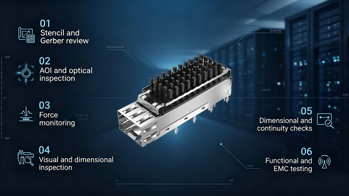
| Assembly stage | Critical control point | Recommended inspection |
|---|---|---|
| PCB stencil design | Press-fit solder paste keep-out | Stencil and Gerber review |
| SMT assembly | LED placement and solder quality | AOI and visual inspection |
| Cage installation | Insertion force and displacement | Force-displacement monitoring |
| Mechanical mounting | Cage seating and coplanarity | Visual and dimensional inspection |
| Front-panel integration | Gasket or spring-finger contact | Dimensional and continuity checks |
| Final validation | LED operation, module fit, and EMI | Functional and EMC testing |
Each stage should have defined acceptance criteria.
For example, press-fit installation should not be accepted solely because the cage appears to be in position. The force profile, seating height, and condition of the PCB mounting holes should also be considered.
Similarly, an EMI gasket should not be approved simply because it is visibly compressed. Its compression range and electrical contact must meet the applicable specifications.
For production consistency, manufacturers should also:
-
Conduct first-article inspection before mass production.
-
Record press-fit force and displacement data.
-
Track recurring dimensional deviations.
-
Maintain traceability for cage and PCB revisions.
-
Establish controlled procedures for extraction and rework.
-
Update DFM rules when a recurring defect is identified.
These practices help convert individual defect corrections into repeatable manufacturing improvements.
Select SFP Cage Assemblies That Match PCB and Chassis Requirements
Choosing the correct SFP cage is an important part of preventing assembly defects. A cage should be evaluated according to its mounting structure, optical configuration, EMI interface, and mechanical compatibility with the target system.
Before selecting an SFP cage assembly, engineers should consider the following parameters:
-
Port configuration: 1x1, 1x2, 1x4, or other available port arrangements.
-
Mounting method: Press-fit, solder-post, or another supported mounting configuration.
-
Light pipe configuration: With or without an integrated light pipe.
-
EMI shielding structure: Spring fingers, conductive gasket, or another specified contact design.
-
PCB requirements: Finished-hole dimensions, board thickness, and mounting footprint.
-
Mechanical dimensions: Cage height, width, length, and front-panel compatibility.
-
Thermal design: Ventilation features or integrated heatsink options.
-
Operating environment: Temperature range and application requirements.
The following examples illustrate how different cage configurations address different PCB integration requirements.
LINK-PP SFP cage assemblies provide several configuration options for networking hardware and PCB integration. Our product range includes single-port and multi-port cage solutions with different mounting, light pipe, EMI shielding, and thermal configurations.
For example:
-
LINK-PP LP11AC02060: A 1x1 SFP cage with press-fit mounting, integrated heatsink, and perimeter EMI spring fingers. Its listed package height is 9.75mm, and its operating temperature range is -55°C to +85°C.
-
LINK-PP LP21AC02301: A 2x1 SFP cage with press-fit termination, an outer light pipe, and EMI spring fingers. Its listed operating temperature range is -40°C to +85°C.
These examples demonstrate why cage selection should be based on the complete assembly requirement rather than port count alone.
The right configuration depends on the PCB footprint, host connector arrangement, LED location, front-panel geometry, and required shielding structure.
When evaluating a LINK-PP SFP cage, engineering teams can use the corresponding product specifications and mechanical drawings to verify the intended application. We recommend checking the exact part number and dimensional documentation before finalizing the PCB layout.
Final SFP Cage Assembly Quality Checklist
A practical inspection checklist helps manufacturing engineers verify that critical assembly requirements have been met before a PCB enters final testing.
The following checklist covers the five major defect categories discussed in this guide.
PCB and press-fit preparation
-
Press-fit holes are free of unintended solder paste.
-
Finished-hole dimensions meet the cage specification.
-
PCB plating and thickness meet the application requirements.
-
Compliant pins are aligned before insertion.
Optical alignment
-
SMD LEDs are positioned correctly.
-
Light pipes are aligned with the LED optical input.
-
No visible light pipe deformation is present.
-
LED illumination and front-panel visibility are verified.
Press-fit installation
-
Insertion force is controlled and recorded.
-
The cage reaches the specified seating depth.
-
No visible pin deformation is present.
-
PCB mounting holes show no signs of mechanical damage.
Mechanical integration
-
The cage sits flat against the PCB.
-
PCB warpage is within the specified limits.
-
Adjacent components and mounting hardware have adequate clearance.
-
Transceiver insertion, latching, and extraction operate correctly.
EMI and front-panel integration
-
Spring fingers or conductive gaskets are correctly positioned.
-
Front-panel contact meets the specified dimensional requirements.
-
Gasket compression is within the manufacturer's specified range.
-
Cage-to-chassis electrical continuity is verified.
-
EMC performance is validated under representative operating conditions.
This checklist can be incorporated into first-article inspection, production quality documentation, and final assembly verification.
The objective is not simply to identify defective cages after installation, but to prevent the conditions that cause those defects in the first place.
Conclusion
SFP cage assembly defects can significantly reduce PCB yield when mechanical, optical, and EMI interfaces are not properly controlled. Solder paste contamination, LED misalignment, uncontrolled press-fit insertion force, improper cage seating, and insufficient panel compression are five critical problems that can lead to PCB damage, functional failures, rework, and unreliable shielding.
Preventing these failures requires attention to both component selection and manufacturing process control.
The most important points are:
-
Press-fit hole contamination: Maintain solder paste keep-out zones and verify PCB hole conditions.
-
Light pipe misalignment: Match LED placement coordinates with the actual cage optical geometry.
-
Uncontrolled insertion force: Use suitable tooling, PCB support fixtures, and force-displacement monitoring.
-
Improper cage seating: Verify pin alignment, PCB flatness, mounting height, and mechanical clearance.
-
Insufficient panel compression: Validate the PCB-to-panel tolerance stack-up and EMI contact requirements.
For manufacturers developing networking switches, routers, and other high-density communication equipment, selecting an appropriately designed SFP cage assembly is just as important as controlling the installation process.
At LINK-PP, we provide SFP cage solutions with different port configurations, press-fit mounting options, light pipe arrangements, EMI shielding structures, and thermal designs. Our goal is to help engineering teams identify suitable cage configurations for their PCB and chassis integration requirements.
If you are evaluating an SFP cage for a new PCB design or looking to improve an existing assembly process, explore the available configurations through the LINK-PP Official Store. You can request samples to verify mechanical fit, press-fit compatibility, LED alignment, and front-panel integration before moving into volume production.
For standard-stock items, LINK-PP offers a 15-day no-reason return or exchange policy. If a product has a quality issue, LINK-PP covers the return shipping cost.
Starting with a sample evaluation is a practical way to validate the component against your actual PCB and chassis design, reduce integration risks, and build a more consistent SFP cage assembly process.