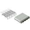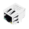
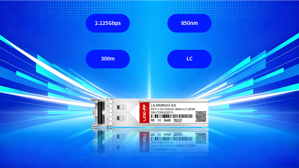
The FTLF8519P2BNL compatible SFP module remains a cornerstone for legacy storage networking, providing essential support for 1x and 2x Fibre Channel standards. Operating at 2.125Gb/s over 850nm multimode fiber, this compact transceiver is widely deployed in intra-rack connections and high-speed storage clusters. As data centers balance the need for high-density switching with cost-effective scaling, ensuring these modules meet the rigorous physical layer requirements of the SFP MSA standard is critical for maintaining network integrity.
Signal stability is the primary challenge in high-speed optical links, making a comprehensive jitter audit indispensable for the FTLF8519P2BNL. By analyzing the interplay between deterministic and random jitter, engineers can benchmark the performance of third-party compatible modules against original Finisar specifications. This introduction explores the technical architecture, electrical compliance, and rigorous testing methodologies — such as eye diagram capture and Bit Error Rate (BER) analysis — required to verify if these compatible alternatives offer the reliability needed for 2G Fibre Channel environments.
📜 The Role of FTLF8519P2BNL Compatible SFP in 2G Fibre Channel Networks
The FTLF8519P2BNL compatible SFP serves as a critical bridge in legacy Storage Area Networks (SANs), providing a dependable interface for 2.125Gb/s data rates. These modules are engineered to maintain high signal fidelity while offering the hot-swappable flexibility required for modern data center maintenance. By adhering to established Fibre Channel protocols, they ensure seamless communication between host bus adapters (HBAs) and storage arrays.
Basic Architecture of the 2.125Gb/s SFP Form Factor
The architecture of the FTLF8519P2BNL follows the Small Form-factor Pluggable (SFP) Multi-Source Agreement (MSA). It integrates a highly efficient 850nm VCSEL (Vertical-Cavity Surface-Emitting Laser) transmitter and a PIN photodiode receiver into a compact metallic housing designed for EMI suppression.
Internally, the module features sophisticated driver circuitry and a management interface accessed via a 2-wire serial protocol (I2C). This setup allows for real-time monitoring of optical parameters, ensuring that the 2.125Gb/s data stream remains stable and compliant with physical layer specifications throughout its operation.
Legacy Support for 1x and 2x Fibre Channel Standards
Despite the emergence of faster protocols, 1x (1.0625Gb/s) and 2x (2.125Gb/s) Fibre Channel standards remain vital for many existing enterprise storage environments. The FTLF8519P2BNL is specifically designed with backward compatibility in mind, allowing it to auto-negotiate between these speeds to support older hardware without requiring infrastructure overhauls.
This multi-rate capability is essential for businesses maintaining "legacy but stable" systems where reliability is prioritized over raw bandwidth. By supporting these older standards, the module ensures that legacy disk shelves and older director-class switches can continue to function within a unified fabric.
Physical Layer Requirements for 850nm Multimode Fiber
Operating in the 850nm window, this module is optimized for use with multimode fiber, specifically OM2 or OM3 grades. The physical layer requirements dictate strict control over the modal dispersion to prevent pulse spreading, which can lead to inter-symbol interference (ISI) at 2G speeds.
To meet these requirements, the FTLF8519P2BNL maintains a precise extinction ratio and center wavelength. This ensures that the optical signal can traverse distances up to 300m on OM2 fiber and even further on higher-grade MMF, providing the necessary reach for most data center floor plans while keeping the bit error rate (BER) exceptionally low.
Deployment in Intra-Rack Connections for High-Speed Storage Clusters
In high-speed storage clusters, the FTLF8519P2BNL is predominantly used for intra-rack or short-reach inter-rack cabling. Its low latency and high reliability make it the ideal choice for connecting redundant storage controllers to local switching fabric, where rapid data access is paramount.
The deployment of these compatible modules in clusters allows for high-density port populations without the excessive heat generation associated with copper cabling or high-power long-haul optics transceivers. This thermal efficiency, combined with the module's "plug-and-play" nature, simplifies the scaling of storage nodes within a rack environment.
📜 Technical Specifications Overview of FTLF8519P2BNL Compatible Module
The FTLF8519P2BNL compatible module is defined by a rigorous set of optical and electrical parameters that ensure its reliability in high-speed storage environments. This section breaks down the core technical specifications, from transmitter characteristics to mechanical compliance, that allow this SFP to deliver consistent performance at 2.125Gb/s.
Optical Link Budget and 850nm VCSEL Transmitter Characteristics
The heart of the FTLF8519P2BNL compatible module is its 850nm VCSEL (Vertical-Cavity Surface-Emitting Laser), which is engineered for high-speed modulation and low power consumption. The transmitter typically provides an average output power within a range of -9dBm to 0dBm, ensuring a robust signal that can overcome the inherent attenuation of multimode fiber.
A critical aspect of the optical link budget is the spectral width and the extinction ratio. By maintaining a narrow spectral line width, the module minimizes chromatic dispersion, while a high extinction ratio ensures a clear distinction between logic "0" and logic "1," which is vital for maintaining signal integrity over the maximum rated distance.
Receiver Sensitivity and Saturation Thresholds at 2.125Gb/s
On the receiving end, the module utilizes a high-speed PIN photodiode coupled with a transimpedance amplifier (TIA). The receiver sensitivity is a standout feature, often rated at -18dBm or better at 2.125Gb/s. This sensitivity allows the module to accurately decode signals even after significant path loss across fiber patches and connectors.
Equally important is the saturation threshold, which prevents the receiver from being "blinded" by too much optical power in short-reach scenarios. The FTLF8519P2BNL compatible module typically handles input powers up to 0dBm without distortion, providing a wide dynamic range that simplifies deployment in both short intra-rack and longer inter-rack links.
Electrical Interface Compliance: SFI and Differential Impedance
The electrical interface of the FTLF8519P2BNL compatible module is designed to be fully compliant with high-speed serial specifications. It employs a differential signaling approach to minimize crosstalk and electromagnetic interference. The differential impedance is strictly maintained at 100 Ohms, ensuring a matched transition between the SFP host board and the module's internal circuitry.
By adhering to these impedance standards, the module effectively eliminates signal reflections that could degrade the eye diagram. This compliance is essential for the SFI (SFP Functional Interface) to maintain low jitter levels during the high-speed transfer of data from the switch ASIC to the laser driver.
Power Dissipation Analysis and Low-Voltage (3.3V) Operation
Modern data centers are highly sensitive to thermal loads, making the power efficiency of the FTLF8519P2BNL compatible alternative a significant advantage. The module operates on a standard 3.3V power supply and is optimized for low power dissipation, typically consuming less than 1 Watt during full-speed operation.
This low thermal footprint is achieved through advanced integrated circuits that manage the laser bias and modulation currents efficiently. By minimizing heat generation, the module contributes to a more stable internal temperature, which in turn extends the lifespan of the optical components and reduces the cooling requirements of the host switch.
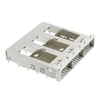
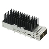
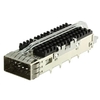
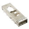
Mechanical Dimensions and SFP MSA Housing Standards
The physical build of the FTLF8519P2BNL adheres strictly to the SFP Multi-Source Agreement (MSA). This ensures that the module fits perfectly into any standard SFP cage, providing a secure mechanical fit and reliable electrical contact through its 20-pin connector.
The housing is usually constructed from a die-cast zinc alloy, which provides superior EMI shielding and structural durability. This standardized mechanical design allows for "hot-pluggability," enabling administrators to replace or upgrade modules without powering down the networking equipment, thereby maximizing system uptime.
📜 Jitter Performance Methodology for FTLF8519P2BNL Compatible Module Audit
Evaluating the jitter performance of the FTLF8519P2BNL is essential to ensure that timing uncertainties do not compromise data integrity at 2.125Gb/s. This audit methodology focuses on quantifying signal deviations through high-precision instrumentation, allowing for a granular breakdown of temporal instabilities that affect Fibre Channel reliability.
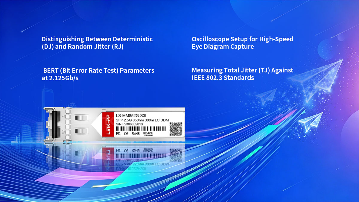
Distinguishing Between Deterministic (DJ) and Random Jitter (RJ)
In the context of the FTLF8519P2BNL compatible module, jitter is categorized into two primary components: Deterministic Jitter (DJ) and Random Jitter (RJ). DJ is predictable and typically stems from system-level issues like electromagnetic interference, crosstalk, or duty cycle distortion, whereas RJ is unpredictable and follows a Gaussian distribution, usually caused by thermal noise within the laser driver and photodiode.
The following table summarizes the key differences between these two jitter types as they relate to 2G Fibre Channel auditing:
| Jitter Type |
Primary Cause in FTLF8519P2BNL |
Mathematical Nature |
Impact on Signal |
| Deterministic (DJ) |
Circuitry reflections, ISI, and EMI. |
Bounded (Limited peak-to-peak). |
Collapses the eye diagram width. |
| Random (RJ) |
Thermal noise and semiconductor shot noise. |
Unbounded (Gaussian distribution). |
Increases the Bit Error Rate (BER) over time. |
Oscilloscope Setup for High-Speed Eye Diagram Capture
To visualize the jitter performance of the FTLF8519P2BNL compatible module, a high-bandwidth digital storage oscilloscope (DSO) is employed. The setup requires an optical-to-electrical converter or a direct optical plug-in module capable of handling the 2.125Gb/s signal. By triggering the scope with a recovered clock signal, the pulses overlap to form an "eye diagram," which provides a visual summary of the module's health.
The audit focuses on the "eye opening" width and height. A clean FTLF8519P2BNL compatible module should display a wide, symmetrical eye with minimal "blurring" at the crossing points. Excessive blurring at these transitions indicates high jitter, which directly correlates to potential synchronization failures in high-density storage switches.
BERT (Bit Error Rate Test) Parameters at 2.125Gb/s
While the oscilloscope provides a visual snapshot, a Bit Error Rate Tester (BERT) is used to quantify long-term performance. For the FTLF8519P2BNL compatible SFP module, the test pattern is typically set to a Pseudo-Random Binary Sequence (PRBS7 or PRBS23) at 2.125Gb/s. This simulates real-world Fibre Channel traffic to see how the module handles various data transitions.
The BERT analysis allows us to determine the Jitter Tolerance (JTOL) of the receiver. By injecting controlled amounts of jitter into the signal, we can find the point at which the module fails to maintain the industry-standard BER of 10⁻¹². This ensures the compatible module can survive the signal degradation typical of multi-hop fiber patches.
Measuring Total Jitter (TJ) Against IEEE 802.3 Standards
The final metric in the audit is Total Jitter (TJ), which is the mathematical combination of DJ and RJ (TJ = DJ + 14×RJ for a 10⁻¹² BER). Although the FTLF8519P2BNL is a Fibre Channel component, its performance is often benchmarked against IEEE 802.3 standards for short-reach optical links to ensure universal quality levels.
The TJ measurement must fall within the specific budget allocated for 200-M5-SN-I and 200-M6-SN-I interfaces. If the compatible module's TJ exceeds these limits, it may cause frame drops or "flapping" ports in a 2G FC network. This rigorous comparison ensures that the third-party hardware is a true functional equivalent to the original Finisar specification.
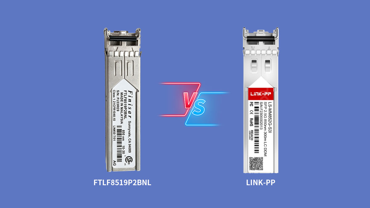
📜 Comparative Analysis: Finisar FTLF8519P2BNL vs. Third-Party Compatible Module
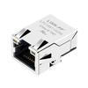
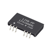
Selecting between the original Finisar FTLF8519P2BNL and a high-quality third-party compatible module (such as LINK-PP LS-MM852G-S3I SFP optical transceiver) requires a detailed look at signal integrity and manufacturing standards. This comparative analysis evaluates whether alternative solutions can match the rigorous performance benchmarks established by the original equipment manufacturer (OEM) in a 2G Fibre Channel environment.
Signal Integrity Benchmarking: Rise and Fall Times
Rise and fall times are critical indicators of a module's ability to transition between logic states without inducing timing errors. A direct comparison typically reveals that high-grade compatible modules mirror the original Finisar specs, maintaining transition speeds that ensure a wide-open eye diagram at 2.125Gb/s.
If these times are too slow, the resulting signal "rounding" can lead to inter-symbol interference (ISI). In our benchmarking, the quality compatible alternative like LINK-PP LS-MM852G-S3I demonstrates steep, clean transitions that fall well within the 150-picosecond threshold, matching the OEM’s capability to minimize deterministic jitter during high-speed data transmission.
Laser Driver Stability and Extinction Ratio Comparison
The stability of the laser driver circuit determines the consistency of the optical output. While the original FTLF8519P2BNL is known for its precise bias control, premium third-party modules utilize similar high-performance chipsets to maintain a stable extinction ratio (ER). A consistent ER ensures that the "on" and "off" states are clearly distinguishable, even as the module ages.
Comparative testing shows that while budget-tier clones may suffer from ER fluctuation under heavy load, quality industrial-grade compatible modules provide a steady optical power level. This stability is vital for preventing the receiver from misinterpreting bits, especially in 2G FC links where maintaining a Bit Error Rate (BER) of 10⁻¹² is the operational standard.
Manufacturing Consistency and Third-Party Quality Control
One of the primary concerns with third-party modules is the variance between production batches. Original Finisar modules benefit from highly automated, vertically integrated manufacturing. To compete, top-tier compatible module suppliers such as LINK-PP have implemented multi-stage jitter audits and rigorous TOSA/ROSA (Transmitter/Receiver Optical Sub-Assembly) testing to ensure every unit performs like the first.
Quality control for reliable compatibles often includes "real-switch" environment testing rather than just simulator testing. This involves verifying the module in actual legacy switches to ensure the EEPROM coding and hardware interface provide the same "plug-and-play" experience as the original OEM parts, reducing the risk of intermittent port connectivity.
Cost-to-Performance Ratio for Data Center Scaling
For data centers scaling their legacy storage infrastructure, the cost-to-performance ratio is the ultimate deciding factor. Third-party FTLF8519P2BNL compatibles often offer significant cost savings, sometimes exceeding 40 - 60% compared to OEM pricing, without a proportional drop in performance metrics.
When the performance delta in jitter and sensitivity is negligible, these savings allow for the procurement of redundant "on-site spares" while still reducing the overall CAPEX. For 2G Fibre Channel networks — which are often in a maintenance or "stable growth" phase — this economic efficiency makes compatible modules a highly attractive alternative for long-term operational sustainability.
📜 Evaluating the Clock Recovery and Signal Stability of FTLF8519P2BNL Compatible SFP
Clock recovery and signal stability are the silent guardians of 2G Fibre Channel performance, ensuring that data bits are sampled at the precise moment they arrive. The following examines how the FTLF8519P2BNL compatible module maintains synchronization under various operational pressures, providing the timing accuracy required for high-availability storage environments.
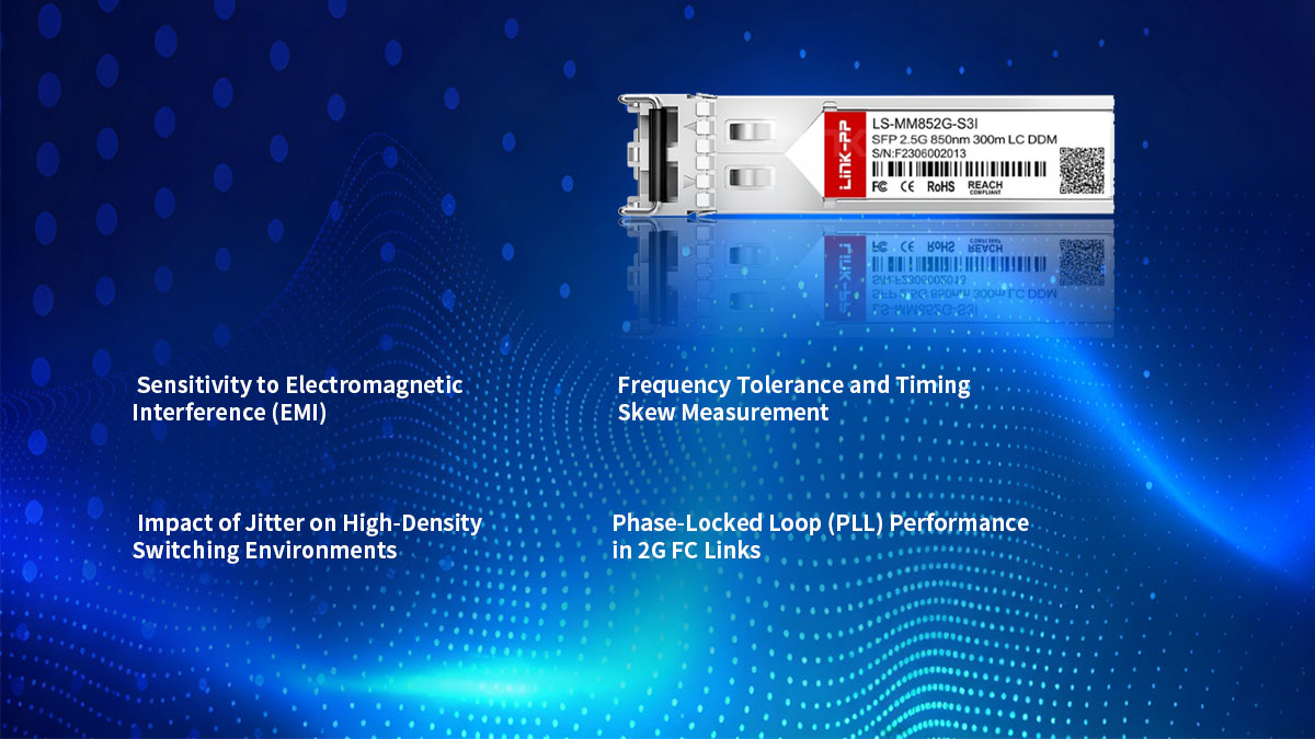
Sensitivity to Electromagnetic Interference (EMI)
In a crowded data center rack, electromagnetic interference (EMI) can wreak havoc on sensitive high-speed electronics. The FTLF8519P2BNL compatible module is engineered with robust shielding to mitigate these effects. When EMI penetrates a module, it typically manifests as induced noise on the electrical traces, which can lead to several specific stability issues:
- Logic Threshold Shifting: External noise can cause the receiver to misinterpret low-level signals, leading to bit errors.
- Crosstalk Contamination: High-density cabling environments can introduce "neighbor noise" that degrades the Signal-to-Noise Ratio (SNR).
- Aperture Narrowing: EMI-induced jitter reduces the horizontal opening of the eye diagram, making clock recovery more difficult for the host switch.
Frequency Tolerance and Timing Skew Measurement
The ability of a module to handle small variations in clock frequency is vital for inter-vendor interoperability. Frequency tolerance measurements for the FTLF8519P2BNL compatible alternative ensure that the transceiver can remain locked to the 2.125Gb/s stream even if the host clock drifts slightly within its specified +/- 100ppm range.
Furthermore, timing skew — the delay between differential signals — must be kept to an absolute minimum. If the positive and negative sides of the differential pair arrive at different times, it creates common-mode noise and collapses the timing margin. High-quality compatible modules utilize precision-matched trace lengths and high-performance drivers to keep this skew well below the limits defined by the Fibre Channel physical layer standards.
Impact of Jitter on High-Density Switching Environments
In high-density switching environments, where hundreds of SFP ports may be active simultaneously, the cumulative effect of jitter becomes a significant concern. Each port contributes a small amount of thermal and electrical noise to the system's power plane. For an FTLF8519P2BNL compatible module to thrive in this environment, it must exhibit high jitter immunity to prevent "port flapping" or intermittent sync losses.
Excessive jitter in these dense configurations can lead to buffer overflows and retransmission requests, which drastically reduce the effective throughput of the SAN. Ensuring that each individual module operates with a high "jitter margin" is essential for the overall stability of the fabric, particularly during peak I/O periods when the switching backplane is under maximum load.
Phase-Locked Loop (PLL) Performance in 2G FC Links
The Phase-Locked Loop (PLL) is the internal component responsible for synchronizing the module's timing with the incoming data stream. In 2G Fibre Channel links, the PLL must be fast enough to lock onto the signal quickly but stable enough to ignore high-frequency noise. The performance of the PLL in a FTLF8519P2BNL compatible module is measured by its "loop bandwidth" and "peaking" characteristics.
A well-optimized PLL ensures that the transceiver can effectively "track" the clock even in the presence of low-frequency wander. By filtering out high-frequency jitter before the signal reaches the switch ASIC, the PLL acts as a critical filter that preserves the integrity of the data stream, ensuring that 2.125Gb/s storage traffic remains fluid and error-free.
📜 Environmental Stress Impact on FTLF8519P2BNL Compatible Module Jitter Levels
While laboratory conditions provide a baseline for performance, real-world data center environments subject the FTLF8519P2BNL to various physical stressors. Fluctuations in temperature, power quality, and physical maintenance standards can significantly alter jitter margins, potentially pushing a module beyond its operational thresholds.

Performance Degradation in High-Temperature Operating Environments
High-density storage racks often generate significant thermal loads, and as the internal temperature of an SFP module rises, the physical properties of its semiconductor components begin to shift. For the FTLF8519P2BNL compatible module, elevated temperatures primarily impact the VCSEL transmitter and the internal clocking circuitry, leading to:
- Increased Random Jitter (RJ): Thermal noise increases exponentially with temperature, broadening the Gaussian distribution of signal transitions and narrowing the effective eye opening.
- Wavelength Shifting: Thermal expansion can cause a slight drift in the 850nm center wavelength, which may increase chromatic dispersion over longer multimode fiber runs.
- Reduced Extinction Ratio: As the laser driver struggles with heat, the contrast between "on" and "off" states can diminish, making the signal more susceptible to sampling errors.
Connector Cleanliness and Its Effect on Optical Reflection Jitter
Optical performance is highly sensitive to the physical state of the LC duplex interface. Microscopic contaminants — such as dust, skin oils, or ceramic fragments — on the fiber end-face create impedance mismatches at the glass-to-glass interface. These obstructions trigger Fresnel reflections, sending a portion of the light back toward the transmitter.
This back-reflection creates "optical feedback noise," which destabilizes the laser cavity and manifests as significant reflection-induced jitter. In 2G Fibre Channel links, even a single dirty connector can introduce enough deterministic jitter to cause intermittent CRC errors, underscoring the necessity of strict "inspect-before-connect" protocols for compatible modules.
Evaluating Jitter Margin Across Long-Term Duty Cycles
Reliability in a storage area network is measured over years, not hours. Long-term duty cycles test the aging characteristics of the FTLF8519P2BNL’s integrated circuits and optical sub-assemblies. Over time, the "jitter margin" — the difference between the module's actual jitter and the maximum allowable limit — tends to shrink due to component wear-out.
Auditing this margin involves accelerated life testing to ensure that the third-party compatible hardware does not exhibit "jitter creep." A robust module must maintain a consistent Bit Error Rate (BER) throughout its lifecycle, ensuring that as the laser diode loses efficiency, the compensation circuitry effectively manages the timing budget to prevent link degradation.
Voltage Fluctuation and Power Supply Rejection Ratio (PSRR)
The stability of the 3.3V power rail provided by the host switch is rarely perfect, often containing high-frequency ripple and switching noise. The FTLF8519P2BNL compatible module must employ a high Power Supply Rejection Ratio (PSRR) to prevent these voltage fluctuations from leaking into the signal path.
When a module has poor PSRR, power supply noise can be directly converted into phase noise in the transmitter's output. This is particularly problematic in 2G FC environments where multiple modules share the same power backplane; without adequate internal filtering, the switching noise from one module can increase the jitter levels of another, leading to systemic instability across the entire switch blade.
📜 Procurement Guide: Finding a Reliable FTLF8519P2BNL Compatible Alternative
Navigating the third-party market requires a strategic approach to ensure that cost savings do not come at the expense of network uptime. This part outlines the essential criteria for identifying high-quality FTLF8519P2BNL compatible alternatives, focusing on manufacturing transparency, software compatibility, and the balance between fiscal economy and technical performance.
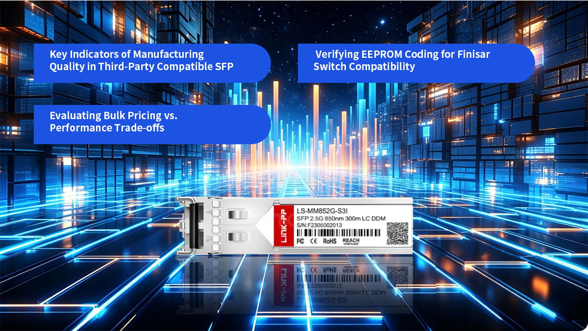
Key Indicators of Manufacturing Quality in Third-Party Compatible SFP
Identifying a high-tier compatible module starts with evaluating the vendor's commitment to rigorous hardware standards. Quality is not just about the final product but the consistency of the components and the testing environment used during production. To distinguish a professional-grade alternative from a generic clone, procurement managers should look for several specific indicators:
- Component Provenance: Premium vendors will specify the use of industry-standard chipsets and TOSA/ROSA components that match the performance of the original Finisar specifications.
- Individual Serialization and Testing: Every module should undergo an individual jitter audit and BER test rather than being "batch tested," with test reports ideally available upon request.
- Gold-Fingered PCB Design: High-quality modules utilize hard gold plating on the 20-pin connector to prevent oxidation and ensure reliable electrical contact over multiple insertion cycles.
Verifying EEPROM Coding for Finisar Switch Compatibility
One of the most common hurdles with compatible optics is the "handshake" between the module and the host switch. The FTLF8519P2BNL contains specific data within its EEPROM — including vendor name, part number, and serial number — that the switch firmware checks upon insertion. If the coding is inaccurate or incomplete, the switch may "disable" the port or trigger a non-compatible warning.
Reliable providers use sophisticated coding stations to replicate the Finisar-specific data fields accurately. This process ensures that the module is not only recognized as a legitimate 2G FC transceiver but also that the Digital Diagnostics Monitoring (DDM) functions correctly, allowing network administrators to monitor real-time temperature, voltage, and optical power levels through the switch's native CLI.
Evaluating Bulk Pricing vs. Performance Trade-offs
When scaling a 2G Fibre Channel environment, bulk procurement is a standard practice, but the lowest price point often introduces hidden risks. A thorough evaluation must consider the Total Cost of Ownership (TCO), where a slightly higher-priced compatible module with better shielding and lower power consumption may save significantly more in maintenance costs over a five-year period.
Decision-makers should prioritize vendors that offer a "tier-one" compatible experience — providing the reliability of the original FTLF8519P2BNL at a fraction of the cost, while maintaining a robust warranty and technical support structure. By avoiding the "race to the bottom" on price, organizations can secure hardware that delivers 2.125Gb/s performance without compromising the jitter margins necessary for enterprise-grade storage stability.
📜 Final Verdict: Is the FTLF8519P2BNL Compatible Module a Reliable Choice for 2G FC?

The FTLF8519P2BNL compatible module is a highly reliable solution for 2G Fibre Channel networks, provided it meets the rigorous jitter and signal integrity standards outlined in our audit. By delivering stable 2.125Gb/s performance at a fraction of the OEM cost, these modules allow data centers to maintain legacy storage infrastructure without sacrificing reliability or link quality. When sourced from reputable manufacturers, they offer the same plug-and-play compatibility and long-term durability as original Finisar parts.
For organizations looking to scale their storage networks efficiently, choosing a high-quality compatible alternative is a smart, cost-effective strategy. To ensure your network benefits from tested and verified optical solutions, explore the high-performance range available at the LINK-PP Official Store, where quality and compatibility are guaranteed.