As data centers race to keep up with the demands of AI and cloud computing, the demand for high-density, high-speed optical connectivity has never been greater. The QDD 400G SR8 transceiver has emerged as a cornerstone technology for short-reach applications, packing an impressive 400Gbps of bandwidth into a compact form factor. This blog will break down how this powerhouse module achieves its massive throughput by combining advanced signaling with high-density fiber interfaces.
At the heart of the QDD 400G SR8’s efficiency is a powerful synergy between PAM4 signaling and the MPO-16 interface. By utilizing 4-level pulse amplitude modulation across 8 parallel channels, the module maps complex data streams directly into a single row of 16 fibers. From the inner workings of PAM4 decoding to physical cabling topologies, we will explore the core specifications and architecture that make this interconnect vital for modern network infrastructure.
✴️ Architectural Integration of PAM4 and MPO-16 in QDD 400G SR8
The seamless fusion of advanced digital signaling and high-density physical interfaces is what allows the QDD 400G SR8 to deliver massive bandwidth within data centers. By pairing a multi-level modulation format with a precise 16-fiber physical connector, the module optimizes both space and spectral efficiency. Understanding this hardware integration reveals how electrical data transforms smoothly into parallel optical streams.
How 8-Lane PAM4 Maps Directly to MPO-16 Fiber Channels
The QDD 400G SR8 architecture relies on an elegant, symmetrical mapping system that pairs eight internal signaling lanes with the physical fibers of an MPO-16 connector. The 16 individual fibers inside the connector are split evenly into two functional groups: eight dedicated fibers for transmitting (Tx) data and eight for receiving (Rx) data.
Each independent PAM4 optical lane is assigned its own dedicated fiber strand within the single-row MPO-16 ferrule. This direct 1:1 hardware mapping eliminates the need for complex internal optical multiplexing components, which significantly lowers the module's overall power consumption, heat dissipation, and manufacturing costs.
Aggregate 400Gbps Throughput: 53.125Gbps per Lane Architecture
To reach a total aggregate throughput of 400Gbps, the transceiver operates eight parallel lanes simultaneously, with each lane carrying a data rate of 53.125Gbps. This specific speed is achieved by running a 26.5625GBaud signaling rate through a 4-level modulation scheme, effectively doubling the bit rate without requiring more physical bandwidth.
When all eight channels transmit data concurrently (8 × 53.125Gbps), the module achieves its full, raw 425Gbps line rate. Once the standard IEEE network overhead and error-correction data are factored in, the system delivers a clean, net throughput of exactly 400Gbps of pure payload data.
The Synergy Between Multi-Level Signaling and Parallel Optics
The true strength of the QDD 400G SR8 lies in the collaborative synergy between multi-level PAM4 signaling and parallel optical design. While PAM4 compresses twice as much data into the electronic and optical components, the parallel layout distributes this dense traffic across eight separate physical paths to prevent data bottlenecks.
If the system relied on older NRZ (2-level) signaling, it would require either 16 separate fibers per direction or double the optical frequency speed, both of which would drastically increase cost and complexity. By combining 4-level states with an organized 16-fiber array, the module achieves the perfect balance of manageable component speeds, high port density, and reliable short-reach performance.
✴️ Optical Transmitter Specs and PAM4 Encoding in QDD 400G SR8
The optical transmitter assembly is the engine that converts electrical bits into precise, high-speed light pulses. By utilizing advanced laser arrays and sophisticated encoding logic, the module ensures high-fidelity data transmission over multimode fiber. Managing these optical parameters accurately is vital for maintaining signal strength and minimizing transmission errors across all parallel channels.
VCSEL Array Modulation Principles for 4-Level Signaling
The QDD 400G SR8 transmitter achieves its high data density by using an array of eight Vertical-Cavity Surface-Emitting Lasers (VCSELs) operating at an 850nm wavelength. Instead of simply turning the lasers on and off, the driver circuit modulates the optical output power into four distinct electrical current levels.
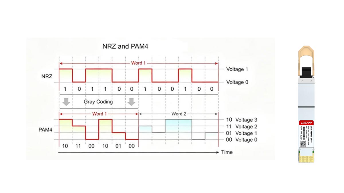
These four discrete levels represent the amplitude states of PAM4 signaling, which are designated as 0, 1, 2, and 3. By varying the laser’s light intensity across these four specific steps, each individual clock cycle (or Baud) successfully transmits two bits of binary data simultaneously instead of just one.
Gray Coding Schemes for Error Reduction in PAM4 Transmitters
Because PAM4 relies on four closely spaced signal levels, a small amount of noise can easily cause a receiver to misidentify a level. To mitigate this risk, the optical transmitter applies a digital logic technique known as Gray Coding to the data stream before modulation.
Gray Coding organizes the data so that adjacent amplitude levels differ by only a single binary bit (for example: 00, 01, 11, 10). Consequently, if a signal drops or spikes into a neighboring level due to link degradation, the system only suffers a 1-bit error rather than a catastrophic 2-bit failure, making error correction much more manageable.
Optical Launch Power Specs Across 8 Parallel Channels
Maintaining a balanced optical launch power across all eight parallel VCSEL channels is critical to ensure uniform signal distribution. Each channel must push out enough optical power to overcome fiber attenuation without overloading the sensitive photodiodes at the receiving end.
Industry standards dictate strict maximum and minimum limits for both average launch power and Outer Optical Modulation Amplitude (OMA Outer). If one channel operates outside these predefined boundaries, it can cause crosstalk or signal drowning, which ultimately destabilizes the entire 400G link.
TDECQ (Transmitter and Dispersion Eye Closure) Metrics for PAM4
Transmitter and Dispersion Eye Closure for PAM4 (TDECQ) is the definitive metric used to evaluate the overall quality of an optical PAM4 transmitter. It mathematically measures the optical power penalty and noise additions caused by transmitter imperfections and multi-mode fiber dispersion.
The following data table outlines the critical transmitter specifications and mandatory TDECQ limits required for stable 400G operation:
| Parameter Specification |
Minimum Value |
Maximum Value |
Unit |
| TDECQ (per Lane) |
— |
4.5 |
dB |
| Average Launch Power (per Lane) |
-6.5 |
4.0 |
dBm |
| Launch Power in OMA Outer (per Lane) |
-4.5 |
3.0 |
dBm |
| Extinction Ratio |
3.0 |
— |
dB |
✴️ Receiver Performance and PAM4 Decoding in QDD 400G SR8
The optical receiver sub-assembly is responsible for capturing incoming light pulses and converting them back into clean electrical signals. Because PAM4 signals are inherently more sensitive to noise than older modulation formats, the receiver must possess exceptional sensitivity and precision. Processing these multi-level incoming signals requires highly accurate alignment and advanced digital decoding mechanisms to ensure data integrity.
Photodiode Array Alignment with MPO-16 Fiber Rows
At the core of the receiver is an integrated array of eight high-speed PIN photodiodes designed to capture incoming optical signals. These photodiodes must align perfectly with the precise physical layout of the single-row MPO-16 connector.
Any microscopic physical misalignment between the internal photodiode surface and the incoming fiber core will cause severe optical insertion loss. To prevent this, the QDD 400G SR8 module utilizes advanced micro-optical lenses to focus the light from each fiber row uniformly onto the active area of the corresponding photodiode channel.
Clock and Data Recovery (CDR) Requirements for 26.5625GBaud PAM4
Once the photodiodes convert the light into electrical currents, the internal Clock and Data Recovery (CDR) circuits take over. Operating at a high symbol rate of 26.5625GBaud, the CDR must lock onto the incoming data stream with absolute precision to sample the signal at the perfect time interval.
Because PAM4 packs more information into the same timeframe, the timing margin is much narrower than traditional NRZ links. The CDR circuit utilizes high-frequency phase-locked loops (PLLs) to minimize phase jitter and accurately track incoming symbol variations across all eight parallel lanes simultaneously.
Receiver Sensitivity Thresholds for 4-Level Amplitude States
Detecting a PAM4 signal requires the receiver to distinguish between four separate amplitude states, which means the signal-to-noise ratio requirements are exceptionally strict. The receiver must feature high input sensitivity to reliably separate these tightly squeezed voltage levels under weak signal conditions.
If the incoming optical modulation amplitude (OMA) drops too low, the boundaries between the four levels become blurry, resulting in bit errors. Transceiver specifications mandate strict minimum sensitivity levels for the optical receiver to ensure it can successfully decode the lowest power states even after fiber attenuation.
Slicing Levels and Adaptive Thresholding for PAM4 Eye Diagrams
To decode a PAM4 eye diagram, the receiver utilizes three separate internal decision thresholds, known as slicing levels, to determine whether a symbol represents a 0, 1, 2, or 3. Because factors like fiber dispersion and thermal noise can distort the signal over time, these slicing levels cannot remain completely fixed.
The receiver employs adaptive thresholding logic that continuously adjusts these decision levels based on real-time signal conditions. The following table highlights the critical slicing and sensitivity metrics required to maintain a clean internal eye diagram:
| Decoding Parameter |
Target Profile / Value |
Operational Function |
| Slicing Threshold Count |
3 Independent Levels |
Separates the 4 amplitude states (0, 1, 2, 3) |
| Threshold Adaptability |
Dynamic / Real-time |
Compensation for asymmetric eye distortion |
| Receiver Sensitivity (OMA Outer) |
-6.5dBm (Maximum) |
Lowest optical power required for reliable decoding |
| Stressed Eye Closure (SECQ) |
4.5dB |
Maximum allowable distortion for input signals |
✴️ Forward Error Correction (FEC) and PAM4 Link Budget for QDD 400G SR8
Because multi-level signaling inherently operates with tighter noise margins, implementing robust mathematical error correction is essential for stable data transmission. Forward Error Correction acts as a safety net, repairing corrupted bits in real time to maintain a highly reliable connection. Carefully managing the optical link budget alongside these digital correction mechanisms ensures that parallel data streams can successfully survive fiber insertion losses.
KP4 FEC (RS-544,514) Mandates for PAM4 Interconnects
The IEEE standards mandate the use of KP4 Forward Error Correction for the QDD 400G SR8 architecture to counteract the high error rates associated with PAM4 signaling. This specific algorithm utilizes a Reed-Solomon RS(544, 514) mathematical formula to embed parity bits directly into the data payload.
The integration of this coding standard introduces several strict system operational parameters:
- Fixed block size: The algorithm processes data in structured frames of 544 symbols.
- Overhead payload requirement: It reserves 30 symbols per frame strictly for error-checking data.
- Correction capability: The system can successfully repair up to 15 corrupted symbols per block.
Pre-FEC vs. Post-FEC Bit Error Rate (BER) Specs for SR8
A healthy 400G SR8 link relies on a dramatic mathematical transformation of data quality between the initial optical reception and the final system output. The raw signal arriving from the multi-mode fiber exhibits a relatively high error rate, which the host system must cleanly eliminate before processing.
The performance boundaries of this digital cleaning process are defined by two strict operational thresholds:
- Maximum Pre-FEC limit: The raw optical input must maintain an error rate better than 2.4 × 10⁻⁴.
- Target Post-FEC threshold: The mathematical engine must reduce the final error rate down to 1.0 × 10⁻¹².
- Flawless payload delivery: Achieving this target ensures virtually zero lost packets for user applications.
Optical Path Penalty (OPP) and Channel Insertion Loss Budgets
The total optical power budget for a multi-mode link must account for both predictable connection losses and unpredictable signal degradation along the fiber path. The Optical Path Penalty (OPP) quantifies the signal-to-noise ratio degradation caused specifically by modal dispersion and reflections.
To ensure the link operates reliably, network designs must balance these penalties against physical hardware losses:
- Maximum channel loss: The total allowable budget for connectors and splices is typically capped at 1.9dB.
- Dispersion allocation: A portion of the power budget is dedicated solely to combating pulse spreading.
- Power margin safety: Maintaining a positive power margin prevents link drops during environmental temperature shifts.
Burst Error Handling in Multi-Level PAM4 Streams
Unlike older signaling formats where errors usually occur in isolation, a single noise spike in a PAM4 system can wipe out multiple consecutive bits. These dense clusters of dropped bits are known as burst errors, and they present a unique challenge to standard correction engines.
The QDD 400G SR8 architecture utilizes specialized data interleaving to distribute and neutralize these concentrated noise hits:
- Symbol distribution: Consecutive bits are scattered across different parallel processing lanes before transmission.
- Error fragmentation: A long burst error is broken into manageable, isolated pieces at the receiver.
- Preventing correction failure: Keeping the errors per block below the maximum threshold prevents total link failure.
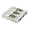
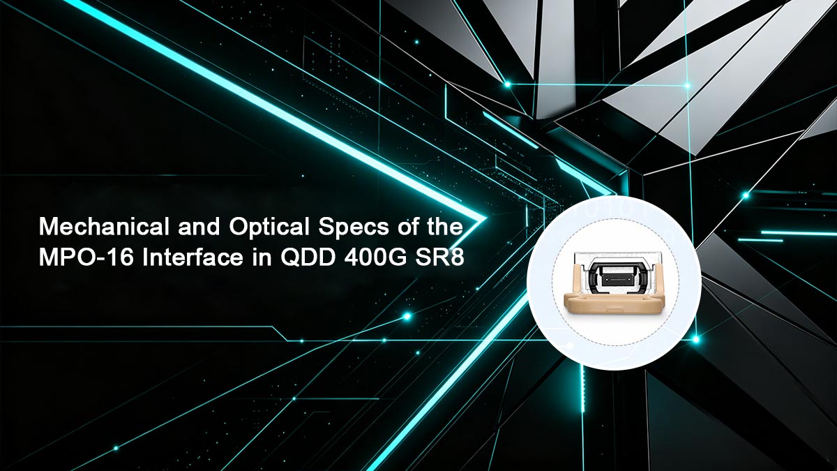
✴️ Mechanical and Optical Specs of the MPO-16 Interface in QDD 400G SR8
The physical reliability of the high-speed optical link depends heavily on the mechanical precision of its connector interface. The MPO-16 system provides the microscopic alignment required to couple light efficiently between the transceiver and the fiber patch cable. Strict adherence to geometric tolerances and polishing standards is essential to maintain low insertion loss across all parallel channels.
MPO-16 Single-Row vs. Legacy MPO-12/24 Ferrule Design
The MPO-16 connector introduces a single-row design specifically optimized for high-density, 8-channel applications. Legacy MPO-12 connectors leave four fibers unused in 8-channel setups, while MPO-24 connectors stack fibers into two distinct rows. This dual-row legacy approach complicates alignment and introduces uneven physical stresses across the connector face.
By contrast, the MPO-16 layout aligns all 16 fibers into a single, highly precise horizontal row. This configuration allows for thinner patch cables and simpler internal routing within the transceiver module. The single-row architecture ensures that every fiber core receives uniform clamping force, dramatically improving link stability.
MPO-16 APC (Angled Physical Contact) 8-Degree Polish Specs
Unlike legacy multi-mode fibers that typically feature flat-polished connectors, the MPO-16 interface utilizes an Angled Physical Contact (APC) finish. The mating surface of the ferrule is polished at a precise 8-degree angle rather than a flat 90-degree plane. This angled design is a critical requirement for managing the tight return loss budgets dictated by PAM4 signaling.
When light hits a boundary gap in a flat connector, the reflected light travels straight back into the VCSEL laser cavity, causing severe timing jitter and signal noise. With an 8-degree APC polish, any back-reflected light is deflected directly into the glass cladding of the fiber instead of returning to the transmitter. This mechanical deflection maximizes return loss and preserves overall signal linearity.
Guide Pin Alignment and Mating Tolerances for High-Density Fiber
To align 16 individual fiber cores simultaneously, the MPO-16 interface relies on a precise male-to-female guide pin mating system. The male connector features two solid metal guide pins protruding from the ferrule, which slide into corresponding alignment holes on the female connector inside the transceiver. The mechanical tolerances for these components are measured at the sub-micron level.
Even a microscopic deviation of 1 to 2 micrometers can shift the fiber cores out of position, causing unacceptable optical attenuation. High-strength internal springs maintain a constant forward pressure when mated, ensuring the fiber faces stay tightly locked together. This continuous physical contact prevents shifting during equipment vibration or temperature fluctuations.
Dust and Contamination Sensitivity on 16-Fiber Faces
The high density of the MPO-16 interface makes it highly vulnerable to dust, oil, and environmental contamination. Because a single-row ferrule holds 16 tightly packed fiber channels, a single microscopic speck of dust can easily block multiple lanes at once. Contamination scatters the light beam, causing localized power drops and bit errors.
Furthermore, if a connector is mated while debris is present, the physical clamping force can permanently scratch or pit the glass surfaces. Regular use of specialized click-cleaners and video inspection probes is mandatory before every insertion. Maintaining absolute cleanliness across all 16 fiber faces is the most effective way to prevent random link degradation.
✴️ Cabling Topologies and Polarity for QDD 400G SR8 MPO-16 Ports
Designing an efficient structured cabling network requires a clear strategy for managing physical fiber routing and channel connectivity. Proper path planning ensures that signals moving through high-density ports arrive at their destinations without overlapping or crossing. Implementing structured alignment standards allows the parallel channels to remain organized and easily scalable across the data center floor.
Pinout Mapping: 8 Tx (Transmit) and 8 Rx (Receive) Lane Positions
The single-row MPO-16 interface organizes its internal fiber channels using a strict spatial layout to guarantee clear separation between signals. Looking at the connector face from left to right, the 16 available positions are split into two equal functional zones. The first eight fiber positions (Fibers 1 through 8) are dedicated entirely to the transmitter (Tx) channels.
The remaining eight fiber positions (Fibers 9 through 16) are reserved strictly for the receiver (Rx) channels. This clean, side-by-side split layout maximizes the physical distance between the active laser arrays and the sensitive photodiodes. By grouping the lanes this way, the module drastically reduces internal optical crosstalk and simplifies internal PCB trace routing.
Type A, Type B, and Type C MPO-16 Polarity Management
Maintaining the correct optical polarity ensures that the transmit (Tx) signals from one transceiver connect directly to the receive (Rx) ports of the opposite module. To achieve this across data center patch panels, standard networks use specific cabling configurations defined as Type A, Type B, or Type C. Each type utilizes a different internal fiber orientation to manage the signal path.
Type A cables use a straight-through mapping where Fiber 1 connects directly to Fiber 1 on the other end, requiring an external flip at the patch panel. Type B cables use a fully inverted "key-up to key-up" layout, shifting Fiber 1 straight to Fiber 16, which is highly popular for direct module-to-module connections. Type C cables pair up adjacent fibers with a simple crossover twist, though this layout is less common in modern 16-fiber parallel optics architectures.
Breakout Configurations: MPO-16 to 2x MPO-8 or 8x Duplex LC
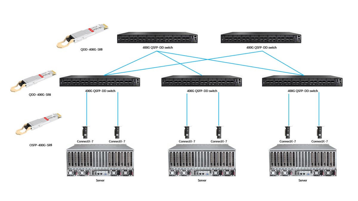
The parallel architecture of the QDD 400G SR8 offers excellent flexibility for channel breakout configurations, allowing a single high-speed port to communicate with multiple lower-speed switches. Using specialized breakout harnesses, the single MPO-16 port can easily split into independent network legs. This capability allows operators to optimize port density and maximize hardware utilization.
One common topology splits the MPO-16 connector into two separate MPO-8 connectors, driving two distinct 200G SR4 modules. Alternatively, the interface can break out into eight individual Duplex LC connections to link directly with legacy 50G server network cards. This granular adaptability makes the module highly effective for both spine-to-leaf switch trunking and direct top-of-rack server distribution.
Maximum Reach Specifications Over OM3, OM4, and OM5 Multi-Mode Fiber
The maximum physical distance a QDD 400G SR8 link can span depends heavily on the grade of multi-mode fiber used in the cabling infrastructure. Because 850nm VCSEL lasers suffer from modal dispersion over distance, higher-grade glass is required to keep the PAM4 eyes open over longer runs. Choosing the correct fiber category prevents inter-symbol interference from degrading the link budget.
When running over standard OM3 fiber, the maximum transmission distance is typically limited to a short 70m. Upgrading the path to OM4 fiber extends this operational reach to 100m, satisfying the layout requirements of most standard data center data halls. For cutting-edge deployments, wideband OM5 fiber supports the same 100-meter reach while providing optimized performance margins against signal dispersion.
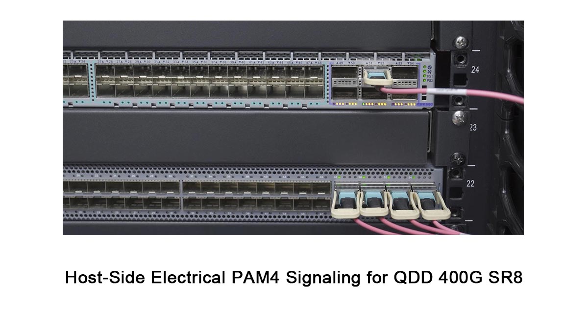
✴️ Host-Side Electrical PAM4 Signaling for QDD 400G SR8
Before data can be converted into light pulses and sent across the fiber network, it must travel cleanly through the electrical copper traces of the host switch. The physical connection between the main system board and the pluggable module relies on highly optimized electrical channels to prevent signal degradation. Ensuring smooth high-frequency data transmission at this stage requires strict equalization standards and rigorous impedance matching.
400GAUI-8 Electrical Interface Specifications
The link between the host switch ASIC and the QDD transceiver chip relies on an industry-standard electrical interface known as 400GAUI-8. This specification defines an 8-lane configuration where each copper lane operates at an electrical throughput rate of 53.125Gbps using PAM4 signaling.
Because the electrical channels mimic the parallel layout of the optical side, the data streams can pass directly through the module with minimal translation latency. The 400GAUI-8 standard enforces strict limits on voltage swings and signal timing margins to guarantee flawless chip-to-module communication.
CTLE and DFE Equalization in the Host-to-Module Path
High-frequency 26GBaud electrical signals degrade rapidly as they travel through the copper traces and connector pins of a switch chassis. To restore these flattened waveforms, the transceiver and host ASIC employ active digital filtering techniques known as Continuous Time Linear Equalization (CTLE) and Decision Feedback Equalization (DFE).
CTLE works at the front end of the receiver path to boost high-frequency signal components while attenuating low-frequency noise. Following that, a multi-tap DFE filter cleans up any remaining inter-symbol interference by predicting and subtracting signal reflections caused by physical trace boundaries.
Channel Operating Margin (COM) for Electrical PAM4 Lanes
Channel Operating Margin (COM) is a comprehensive mathematical metric used to evaluate the overall health and safety margin of an electrical signaling path. Instead of measuring individual performance parameters in isolation, the COM algorithm calculates the ratio of available signal amplitude to total channel noise.
A minimum COM threshold of 3dB is required to ensure an electrical lane can reliably support PAM4 data transmission without dropping packets. This calculation factors in multiple combined penalties, including crosstalk, random jitter, and board material losses, giving engineers a single passing grade for the entire copper channel.
Differential Impedance and Return Loss Mask Compliance
To prevent high-frequency electrical energy from bouncing backward toward the host ASIC, the copper traces must maintain a highly consistent physical structure. The system architecture mandates a strict differential impedance target of 100 ohms across all circuit boards, golden fingers, and connector pins.
Any physical mismatch or manufacturing variation in this impedance profile will trigger signal reflections, causing data distortion and eye closure. Designers must pass strict return loss mask compliance tests to prove that reflected energy levels remain safely below industry-allowed maximums.
✴️ Diagnostic Monitoring of PAM4 and MPO-16 Lanes in QDD 400G SR8
Real-time visibility into telemetry data is essential for maintaining network uptime and identifying localized hardware degradation before it triggers a complete system failure. Integrated telemetry circuitry continuously tracks critical performance metrics across all parallel channels simultaneously. Accessing this localized diagnostic data allows data center engineers to proactively manage link health and accurately isolate physical layer issues.

Per-Lane Real-Time Optical Power Monitoring via DDM
Digital Diagnostics Monitoring (DDM) tracks the optical health of the module by sampling the average incoming and outgoing light levels across all eight parallel lanes individually. Internal circuitry monitors the exact Receive (Rx) and Transmit (Tx) optical power in decibels (dBm), allowing the host switch to instantly detect bent patch cables or misaligned MPO-16 connectors.
Laser Bias Current Tracking for Individual PAM4 Channels
The driver circuit monitors the exact milliampere bias current supplied to each individual VCSEL in the transmitter array to ensure proper light emission. Because PAM4 signaling relies on precise electrical steps to form stable amplitude states, a sudden spike or drop in bias current can instantly flatten the three eye openings, making early tracking vital for discovering aging or faulty lasers.
Temperature and Voltage Effects on PAM4 Signal Linearity
Fluctuations in internal operating temperature and voltage rails can severely distort the linearity of multi-level PAM4 waveforms. Excessive ambient heat shifts the laser's output wavelength, while voltage ripples introduce amplitude noise that causes the slicing levels to misread data. Real-time telemetry continuously charts these environmental changes so the transceiver can dynamically adjust its internal driver settings.
Register Mapping for Lane-Specific Interrupts and Flags
The internal memory structure of the transceiver features a highly organized register map that captures lane-specific interrupt signals and threshold flags. If a specific channel violates preset optical power or temperature boundaries, a dedicated bits/flags register trips, instantly alerting the host software to isolate the exact failing lane without interrupting traffic on the other healthy paths.
✴️ Final Technical Overview of QDD 400G SR8 PAM4 and MPO-16 Specs
The QDD 400G SR8 transceiver represents a monumental leap in short-reach data center connectivity by perfectly harmonizing high-speed digital intelligence with advanced physical engineering. By combining the data-doubling efficiency of 8-lane PAM4 signaling with the streamlined physical footprint of the single-row MPO-16 interface, this architecture delivers maximum density and cost-effective aggregate throughput. From robust host-side equalization and mathematical KP4 FEC error correction to real-time lane monitoring, every technical specification works together to guarantee stable, high-fidelity performance.
Building a dependable, future-proof network infrastructure requires choosing high-quality hardware that strictly adheres to these rigorous optical standards. If you are ready to upgrade your data center interconnects with top-tier reliability and precise mechanical compliance, explore the high-performance 400G QSFP-DD optical transceiver solutions available at the LINK-PP Official Store. Their industry-proven modules deliver the precise signal integrity and seamless port compatibility your high-density 400G infrastructure demands.