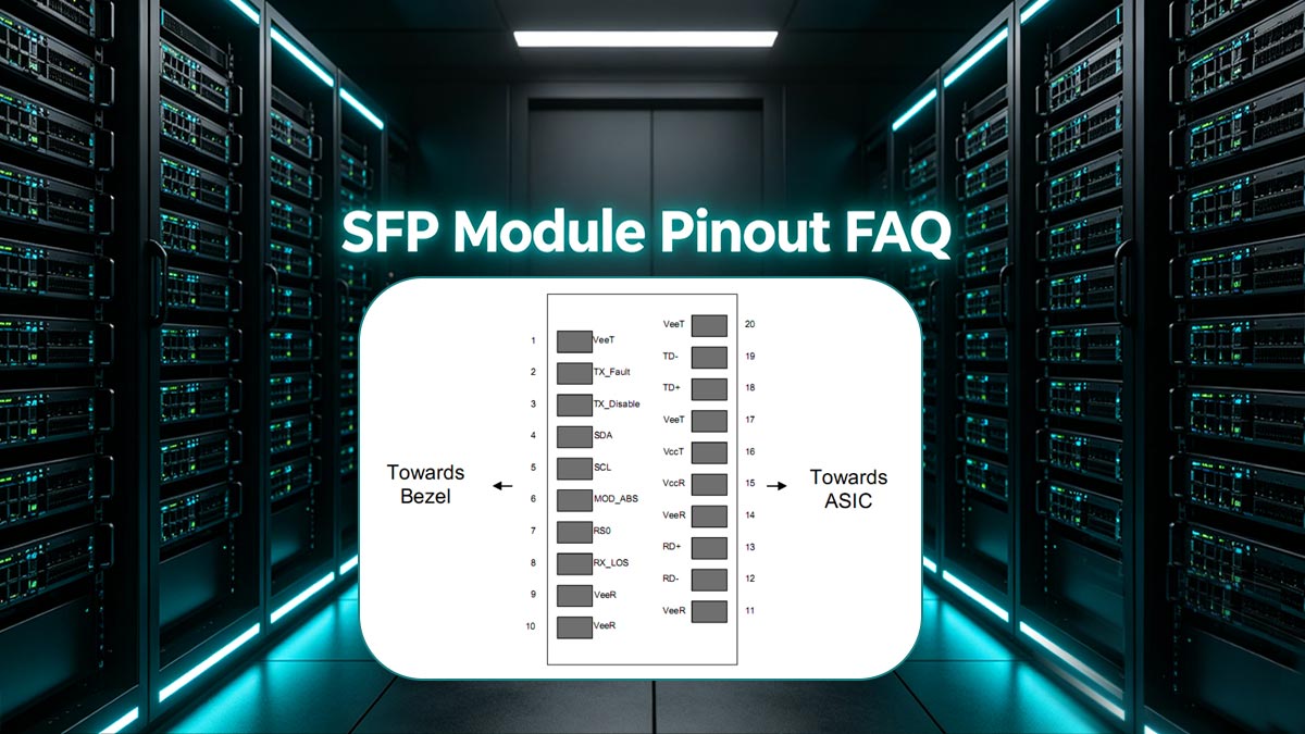
The SFP module pinout is a standardized 20-pin electrical interface defined by the SFF Committee’s INF-8074i Multi-Source Agreement (MSA). It enables hot-pluggable communication between an optical transceiver and a host board, integrating high-speed differential data pairs (TX/RX), 3.3V DC power rails, and a 2-wire I2C management interface for EEPROM access and digital diagnostics.
Whether you are a PCB designer integrating an SFP cage into a custom host board, or a network engineer attempting to flash a generic transceiver to bypass vendor-locked switches, understanding the precise electrical interface is mandatory. Relying on guesswork with optical transceivers can result in fried logic boards, permanently damaged laser drivers, or persistent "Err-Disable" switch port states.
Unlike proprietary hardware, the Small Form-factor Pluggable (SFP) interface relies on an open industry consensus. By mastering this 20-pin layout, you unlock the ability to diagnose physical layer failures at the voltage level and manipulate the module's firmware. This guide breaks down the physical pin mapping, electrical tolerances, and specific I2C addressing protocols required for advanced hardware design and EEPROM reprogramming.
🟢 What Is the SFP Module Pinout? (MSA Standards Explained)
The SFP pinout is the physical and electrical blueprint dictated by the INF-8074i MSA standard. It guarantees hardware interoperability across different networking vendors by standardizing a 20-contact edge connector for data transmission, power delivery, and low-speed module control.
The success of the SFP transceiver in modern fiber optic networking stems entirely from its standardization. The physical dimensions and electrical connections are not owned by equipment giants like Cisco, Juniper, or Arista. Instead, they are governed by a Multi-Source Agreement (MSA)—a collaborative framework established by the SFF (Small Form Factor) Committee.
To ensure absolute interoperability, the MSA standard strictly defines how the module processes electrical signals (electrons) before converting them into optical signals (photons). When analyzing the SFP pinout, hardware engineers must reference two critical documents:
- INF-8074i: The foundational specification that defines the mechanical dimensions, the 20-pin electrical interface, and the basic memory map (I2C address
0xA0).
- SFF-8472: The subsequent extension that defines the Digital Diagnostic Monitoring Interface (DDMI/DOM), mapping real-time temperature, voltage, and optical power data to I2C address
0xA2.
Understanding these standards is the first step in reading the pinout. Every standard SFP module features an identical 20-contact printed circuit board (PCB) edge connector at its rear, carefully engineered to separate high-frequency data lines from low-speed diagnostic logic.
🟢 The Complete 20-Pin SFP Pinout Table: Names and Functions
The 20-pin SFP interface is categorized into four distinct electrical domains: Ground (VeeT/VeeR), Power Supply (VccT/VccR at +3.3V), Low-Speed Control/Status (I2C, TX_Fault, LOS via LVTTL), and High-Speed Data (TD±, RD± via LVPECL). According to the MSA standard, specific ground pins are physically longer to enable safe hot-swapping.
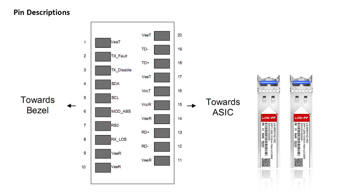
For hardware design, custom PCB routing, and rapid physical-layer troubleshooting, an exact mapping of the SFP edge connector is required. The INF-8074i standard mandates a specific sequence to ensure high-speed signal integrity and prevent power surges during insertion.
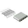
When observing the host board receptacle or the transceiver's PCB edge connector, it is critical to identify the correct orientation. Pin 1 is conventionally located at the bottom-right of the module's PCB trace. Below is the definitive SFP 20-pin reference table, detailing the symbol, logic protocol, and specific function for each contact:
| Pin # |
Symbol |
Logic/Protocol |
Description & Function |
| 1 |
VeeT |
Ground |
Transmitter Ground. (Note: Physically longer pin to engage ground before power during hot-plugging). |
| 2 |
TX_Fault |
LVTTL-O |
Transmitter Fault Indication. A high logic level indicates a laser fault or catastrophic module error. Requires host pull-up resistor. |
| 3 |
TX_Disable |
LVTTL-I |
Transmitter Disable. Driving this pin High (>2.0V) shuts down the optical laser output. |
| 4 |
MOD_DEF(2) / SDA |
I2C |
Module Definition 2 (Serial Data Line). Used for 2-wire I2C communication to read/write the EEPROM. |
| 5 |
MOD_DEF(1) / SCL |
I2C |
Module Definition 1 (Serial Clock Line). Used for 2-wire I2C communication. |
| 6 |
MOD_DEF(0) / Mod_ABS |
LVTTL-O |
Module Absent/Present. Internally grounded within the module. The host board pulls this high; if it reads low, a module is inserted. |
| 7 |
Rate Select |
LVTTL-I |
Bandwidth Selection. Used in multi-rate modules (e.g., Fibre Channel/Gigabit Ethernet switching). Often unconnected in standard 1G optics. |
| 8 |
LOS |
LVTTL-O |
Loss of Signal. A high logic level indicates the received optical power is below the worst-case receiver sensitivity (fiber cut or dirty lens). |
| 9 |
VeeR |
Ground |
Receiver Ground. |
| 10 |
VeeR |
Ground |
Receiver Ground. (Long pin for hot-swap). |
| 11 |
VeeR |
Ground |
Receiver Ground. (Long pin for hot-swap). |
| 12 |
RD- |
LVPECL |
Receiver Inverted Data Output. High-speed AC-coupled differential trace. |
| 13 |
RD+ |
LVPECL |
Receiver Non-Inverted Data Output. High-speed AC-coupled differential trace. |
| 14 |
VeeR |
Ground |
Receiver Ground. |
| 15 |
VccR |
Power |
Receiver Power Supply. Requires clean +3.3V DC (± 5%). |
| 16 |
VccT |
Power |
Transmitter Power Supply. Requires clean +3.3V DC (± 5%). |
| 17 |
VeeT |
Ground |
Transmitter Ground. |
| 18 |
TD+ |
LVPECL |
Transmitter Non-Inverted Data Input. High-speed AC-coupled differential trace. |
| 19 |
TD- |
LVPECL |
Transmitter Inverted Data Input. High-speed AC-coupled differential trace. |
| 20 |
VeeT |
Ground |
Transmitter Ground. (Long pin for hot-swap). |
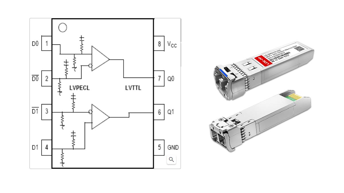
LVPECL vs. LVTTL
Throughout the table, you will notice two primary logic protocols. LVTTL (Low-Voltage Transistor-Transistor Logic) is used for low-speed management and status reporting (Pins 2, 3, 6, 7, 8). Conversely, LVPECL (Low-Voltage Positive Emitter-Coupled Logic) is deployed exclusively for the high-speed data transmission lanes (Pins 12, 13, 18, 19) because its differential nature provides superior electromagnetic interference (EMI) rejection at Gigabit frequencies.
🟢 SFP Electrical Interface Explained
The SFP electrical interface operates across three distinct domains: a strict +3.3V DC power supply (separated into transmitter and receiver rails for noise reduction), high-speed differential pairs (AC-coupled LVPECL/CML) for gigabit data transmission, and low-speed LVTTL logic for host management and status reporting. Maintaining strict impedance and voltage stability across these domains is critical for link reliability.
Understanding the SFP pinout table is only half the battle. To successfully integrate an SFP cage into a custom PCB or diagnose complex physical layer drops, network engineers and hardware designers must understand how these pins behave electrically. The INF-8074i MSA specification mandates strict electrical tolerances to ensure the highly sensitive optical components (lasers and photodiodes) function without electromagnetic interference (EMI).
The 20-pin interface is fundamentally divided into three electrical subsystems: power delivery, high-speed data planes, and low-speed control logic.
1. Power Delivery and Filtering Requirements (+3.3V)
Unlike older GBIC modules that required 5V, the SFP standard operates entirely on a +3.3V DC supply voltage (± 5% tolerance). Power is delivered through Pin 15 (VccR) for the receiver and Pin 16 (VccT) for the transmitter.
Hardware Design Insight: Why does the MSA separate the transmitter and receiver power rails? The optical laser driver (TX) is an electrically noisy component that draws sudden bursts of current. If it shared a direct power trace with the Receiver Optical Subassembly (ROSA), the electrical ripple would distort the incredibly faint micro-amp currents generated by the receiving photodiode, causing massive packet loss. To mitigate this, host boards must implement independent LC (Inductor-Capacitor) filter networks on both the VccT and VccR traces to guarantee a clean, isolated power supply.
2. High-Speed Differential Signaling (AC-Coupled Logic)
The actual network traffic—the gigabits of data flowing in and out of the switch—travels exclusively over Pins 12/13 (RD±) and Pins 18/19 (TD±). Because single-ended traces cannot handle gigabit frequencies without radiating severe EMI, the SFP interface utilizes differential signaling.
- Impedance Matching: On the host PCB, these TX and RX traces must be routed as 100-ohm differential pairs. Any deviation in trace width or spacing will cause signal reflections, degrading the "eye diagram" (signal integrity) and increasing the Bit Error Rate (BER).
- AC Coupling: The high-speed data lines are AC-coupled. This means capacitors (typically 0.1µF) are placed in series with the data traces to block DC voltage, allowing only the high-frequency AC data signal to pass. The MSA standard dictates that the AC coupling capacitors for the transmitter inputs are typically located inside the SFP module, while the receiver outputs must be AC-coupled on the host board.
- Protocol: While historically defined as LVPECL (Low-Voltage Positive Emitter-Coupled Logic), modern module internals often utilize CML (Current Mode Logic). Both protocols rely on a voltage differential between the positive and negative traces to represent binary 1s and 0s, ensuring exceptional common-mode noise rejection.
3. Low-Speed Management Logic (LVTTL & Pull-Ups)
The remaining functional pins—such as TX_Fault (Pin 2), TX_Disable (Pin 3), and LOS (Pin 8)—operate on LVTTL (Low-Voltage Transistor-Transistor Logic). These operate as simple high/low binary switches to communicate module status to the host switch ASIC.
The Role of Pull-Up Resistors: To prevent floating voltage values that could cause false alarms, the MSA requires the host board to pull these status lines up to VccT or VccR using resistors ranging from 4.7kΩ to 10kΩ.
Example: The LOS (Loss of Signal) pin features an open-collector output. During normal operation, the module's internal circuitry pulls the voltage down to ground (0V, or Logic Low). If the fiber optic cable is cut, the photodiode detects no light, the module releases the pin, and the host board's pull-up resistor immediately snaps the voltage up to 3.3V (Logic High), instantly alerting the switch operating system to shut down the port.
🟢 I2C Standards: Locating Pins for EEPROM Flashing
To read or flash an SFP module's EEPROM, you must connect to its 2-wire I2C interface via Pin 4 (SDA - Serial Data) and Pin 5 (SCL - Serial Clock). The module's base identification data (Vendor ID, Part Number) is located at I2C address 0xA0, while real-time optical diagnostics (DDM/DOM) are accessed at address 0xA2.
One of the most highly sought-after applications of the SFP pinout is EEPROM reprogramming. Major networking vendors (such as Cisco, HP, and Arista) frequently implement "vendor locking." When a transceiver is inserted, the host switch's operating system queries the SFP via the I2C bus. If the vendor signature in the EEPROM does not match the switch's proprietary whitelist, the port is forced into an "Err-Disable" state.

For homelabbers, network technicians, and independent hardware developers, bypassing this restriction requires flashing the SFP’s internal memory. This is achieved through the standard I2C (Inter-Integrated Circuit) protocol.
The I2C Pin Mapping
The SFF Committee allocated two specific pins for low-speed serial communication:
- Pin 4: MOD_DEF(2) / SDA: This is the Serial Data Line. It acts as the bidirectional pathway for reading and writing hexadecimal values to the module's EEPROM.
- Pin 5: MOD_DEF(1) / SCL: This is the Serial Clock Line. The host device (e.g., your switch, or a custom Raspberry Pi/Arduino flasher) generates the clock signal to synchronize the data transfer.
Micro-Definition: I2C (Inter-Integrated Circuit): I2C is a synchronous, multi-master, multi-slave packet-switched serial communication bus invented by Philips Semiconductor. It is globally adopted for attaching lower-speed peripheral ICs to processors and microcontrollers over short distances.
SFP Memory Map: 0xA0 vs. 0xA2
When you scan the I2C bus of an active SFP module, you will typically discover two primary device addresses. Understanding the difference between these two memory maps is crucial for successful flashing:
| I2C Address |
Governing Standard |
Data Contained |
Read/Write Status |
| 0xA0 (Base ID) |
INF-8074i |
Vendor Name, OUI (Organizationally Unique Identifier), Part Number, Serial Number, Supported Wavelength, and Link Distance. |
Read/Write (Writing requires overcoming vendor-specific password protection on some modules). |
| 0xA2 (Diagnostics) |
SFF-8472 |
DDM/DOM Data: Real-time Transceiver Temperature, TX Bias Current, TX Output Power, RX Input Power, and Supply Voltage. |
Read-Only (Values are dynamically updated by the module's internal microcontroller). |
*Technical Note: In 7-bit I2C addressing (commonly used by Arduino libraries), 0xA0 and 0xA2 translate to 0x50 and 0x51, respectively.
Expert Insight: DIY EEPROM Flashing Hardware
If you are building a custom rig to flash SFP modules using a microcontroller (like a Raspberry Pi or ESP32), you must adhere to strict electrical rules to prevent hardware damage:
- Use 3.3V Logic Only: The SFP I2C bus is strictly rated for 3.3V. If you use a 5V microcontroller (like a standard Arduino UNO) without a bidirectional logic level shifter, you will instantly fry the transceiver's EEPROM.
- Implement Pull-Up Resistors: The SDA and SCL lines are open-drain. Your flasher circuit must include pull-up resistors (typically 4.7kΩ to 10kΩ) tied to the 3.3V rail to pull the bus high when idle.
- Ground Mod_ABS: If you are testing the SFP outside of a standard cage, ensure you tie Pin 6 (Mod_ABS) to ground. Some modules will not initialize their I2C interface if they believe they are physically floating.
🟢 How to Read an SFP Pinout for Hardware Design
For hardware engineers designing a PCB with an SFP receptacle, reading the pinout requires spatial and electrical planning. Key MSA design rules mandate routing the TX/RX traces (Pins 12/13, 18/19) as strictly matched 100-ohm differential pairs, implementing host-side pull-up resistors (4.7kΩ–10kΩ) for LVTTL control pins, and leveraging the staggered mechanical lengths of ground pins (1, 10, 11, 20) to safely manage Electrostatic Discharge (ESD) during live insertion.

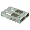
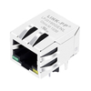
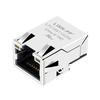
Translating the INF-8074i SFP pinout from a theoretical table into a functional printed circuit board (PCB) requires strict adherence to signal integrity rules. A hardware designer is not just connecting wires; they are managing high-frequency electromagnetic fields. When integrating a 20-pin Surface Mount Technology (SMT) receptacle and the surrounding metallic SFP cage onto a host board, three critical engineering domains must be addressed.
1. The Mechanics of Hot-Swapping (Staggered Pins)
One of the most profound design features of the SFP standard is its native support for hot-swapping—inserting or removing the transceiver while the host switch remains powered on. This is achieved through the physical geometry of the module's PCB edge connector, not software.
- The Mating Sequence: Look closely at the golden contacts on an SFP module. The ground pads (Pins 1, 10, 11, and 20) are physically longer than the power and data pads.
- Electrical Protection: When the module slides into the host receptacle, these ground pins make contact milliseconds before the 3.3V power (Pins 15, 16) or data lines. This establishes a common 0V reference and safely discharges any accumulated Electrostatic Discharge (ESD) into the chassis ground, protecting the delicate switch ASIC and the module's laser driver from fatal voltage spikes.
2. PCB Routing for High-Speed Data Lanes
The gigabit traffic flowing through the transmission (TD±) and receiver (RD±) pins is highly susceptible to attenuation, crosstalk, and impedance mismatches. Hardware designers must treat Pins 12, 13, 18, and 19 with extreme care.
Differential Impedance: Differential impedance is the total opposition to alternating current (AC) flow across a pair of coupled traces. In SFP design, maintaining a continuous 100Ω differential impedance prevents high-speed signal reflections that cause packet loss.
Strict Routing Rules for Host Boards:
- 100Ω Target: The TD± and RD± traces must be routed as tightly coupled differential pairs with a target differential impedance of exactly 100 ohms (± 10%).
- Length Matching: The trace lengths within a single differential pair (e.g., TD+ and TD-) must be perfectly matched—typically within 5 mils (0.127 mm). Any skew between the positive and negative signals will degrade the "eye diagram" and increase the Bit Error Rate (BER).
- Avoid Vias: Routing these high-speed traces through PCB vias creates impedance discontinuities. Keep the TX and RX routing entirely on the top signal layer between the SFP receptacle and the physical layer (PHY) chip whenever possible.
3. SFP Cage Grounding and EMI Shielding
While the 20-pin connector handles the electrical logic, the metallic SFP cage surrounding the module is equally critical for hardware design. At 1.25 Gbps (Gigabit Ethernet) or 10 Gbps (SFP+), the transceiver acts like a broadcasting antenna.
To comply with FCC and CE electromagnetic interference (EMI) regulations, the physical SFP cage must be tied directly to the chassis ground (not the signal ground of the PCB). This is typically achieved using press-fit pins on the cage that connect to grounded plated through-holes (PTH) on the PCB, effectively trapping high-frequency radiation inside the metal housing.
Hardware Design Checklist: Common Pitfalls
| ❌ Poor Practice: |
Floating control pins. Leaving TX_Disable (Pin 3) unconnected can cause unpredictable laser behavior. |
| ✅ Best Practice: |
Implement 4.7kΩ to 10kΩ pull-up resistors to the +3.3V rail for all LVTTL inputs/outputs (Pins 2, 3, 4, 5, 6, 8) on the host PCB. |
| ❌ Poor Practice: |
Routing power (3.3V) to Pins 15 and 16 using a single, unfiltered trace. |
| ✅ Best Practice: |
Deploy independent Pi-filters (inductor flanked by capacitors) for VccT and VccR to isolate the highly sensitive receiver from transmitter switching noise. |
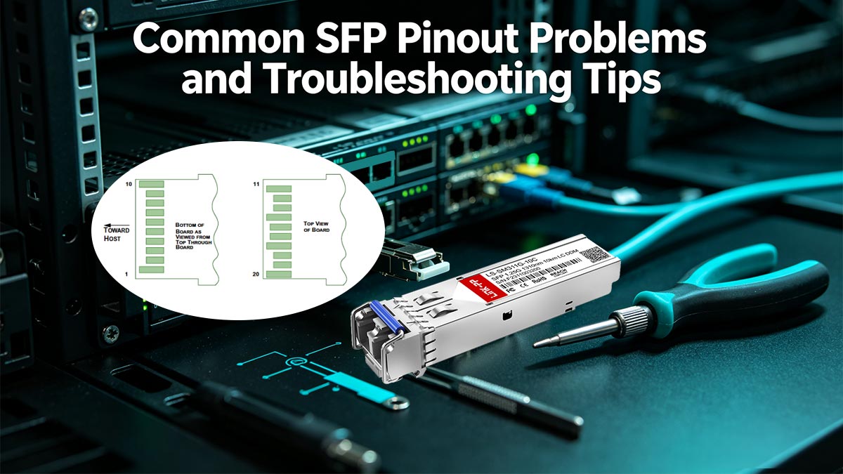
🟢 Common SFP Pinout Problems and Troubleshooting Tips
When an SFP link fails, hardware-level troubleshooting involves reading the LVTTL status pins. A high signal on Pin 8 (LOS) indicates a broken fiber or dirty connector (insufficient light). A high signal on Pin 2 (TX_Fault) means the internal laser has failed or overheated. If the port stays down without a fault, ensure Pin 3 (TX_Disable) is not being erroneously driven high by the host, which forces the laser off.
When a fiber optic link drops, network administrators typically rely on software diagnostics like CLI commands (e.g., show interfaces transceiver). However, software can only report what the hardware pins allow it to see. If an SFP port is stuck in an "Err-Disable" state or fails to link up, understanding the SFP pinout allows you to diagnose the root cause at the physical layer.
Below are the most common SFP hardware failures, mapped directly to their corresponding pins, and actionable troubleshooting steps.
1. The Link is Down, and the Switch Reports "No Signal" (Pin 8: LOS)
The Loss of Signal (LOS) pin is an open-collector output that serves as the transceiver's primary alarm. Under normal operating conditions, the module pulls Pin 8 down to 0V (Logic Low). If the receiving photodiode detects that incoming optical power has dropped below the module's minimum receiver sensitivity threshold, the module releases the pin, and the host board's pull-up resistor snaps it to +3.3V (Logic High).
- Root Cause: The transceiver is not receiving enough light to interpret data.
- Troubleshooting Action:
- Physically inspect the fiber patch cable for severe bends (macro-bending) or breaks.
- Use a fiber optic cleaning pen on both the LC connectors and the transceiver lenses. Over 80% of LOS errors are caused by microscopic dust blocking the optical path.
- Ensure the remote switch is powered on and transmitting.
2. The Port is "Err-Disabled" or Faulted (Pin 2: TX_Fault)
The TX_Fault pin is a critical safety mechanism. Like LOS, it operates via an active-high logic state. If Pin 2 jumps to 3.3V, the SFP module is explicitly telling the host switch: "My internal transmitter hardware has suffered a catastrophic failure."
- Root Cause: This is almost exclusively a hardware failure within the module itself. It typically indicates that the laser diode has degraded, the internal bias current has exceeded safe limits, or the module is severely overheating.
- Troubleshooting Action:
- Remove the SFP module and let it cool. Overheating (especially in densely packed 48-port switches) can trigger a temporary TX_Fault.
- If the fault persists after reinsertion, the module is permanently damaged and must be replaced.
3. Module is Recognized, But Will Not Transmit (Pin 3: TX_Disable)
Unlike LOS and TX_Fault, which are outputs from the module, TX_Disable is an input controlled by the host switch. If the host drives Pin 3 high (>2.0V), the SFP's laser driver is immediately shut down. The module will still be recognized by the switch, and you can still read its EEPROM, but no light will emit from the TX port.
- Root Cause: The switch operating system has intentionally disabled the port, or there is a hardware logic error on the host board.
- Troubleshooting Action:
- Check the switch configuration. Is the interface administratively shut down (e.g., shutdown command in Cisco IOS)?
- If you are building custom hardware, ensure you have not accidentally left Pin 3 floating or tied to 3.3V. It must be pulled low (to Ground) for the laser to fire.
4. The Switch Says "No Transceiver Inserted" (Pin 6: Mod_ABS)
If you plug an SFP into a switch and nothing happens—no logs, no lights, no EEPROM data—the host board does not realize a module is present. This detection relies entirely on Pin 6 (Mod_ABS - Module Absent).
- Root Cause: Inside every standard SFP, Pin 6 is permanently hardwired directly to the ground pins (VeeT/VeeR). The host switch pulls its corresponding receptacle pin up to 3.3V. When you insert the SFP, the module physically bridges that connection to ground, dropping the voltage to 0V and triggering the switch's insertion interrupt.
- Troubleshooting Action:
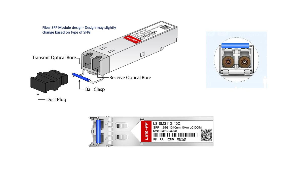
- The module might not be fully seated. Push firmly until the bail clasp clicks.
- Inspect the golden edge connector on the SFP. If Pin 6 is scratched or oxidized, it cannot establish a ground connection. Clean the contacts with isopropyl alcohol.
🟢 SFP vs. SFP+ Pinout: What Is the Difference?
Physically and electrically, the 1G SFP and 10G SFP+ pinouts are virtually identical, both utilizing the exact same 20-pin MSA layout. The difference lies strictly in the engineering of the high-speed data pins (12/13 and 18/19), where SFP+ requires significantly tighter impedance control and higher quality PCB materials to handle 10 Gbps frequencies without severe signal degradation.
One of the most frequent questions encountered when dealing with fiber optic hardware is whether SFP (1 Gigabit) and SFP+ (10 Gigabit) modules share the same pinout. Because they look identical to the naked eye, network administrators often wonder if they can mix and match these optics within different switch ports.

The short answer is yes, they share the exact same 20-pin mapping. The SFF Committee intentionally designed the SFF-8431 standard (governing SFP+) to be backward compatible with the older INF-8074i standard (governing SFP). However, identical physical pins do not guarantee identical electrical performance.
What Stays the Same?
If you plug a 10G SFP+ module into a 1G SFP port, or vice versa, the pins will align perfectly. The underlying control logic remains unchanged:
- Power Delivery: Both modules require exactly +3.3V DC on Pins 15 and 16.
- Management Interface: Both utilize Pins 4 (SDA) and 5 (SCL) for I2C communication, allowing the switch to read the EEPROM at address 0xA0 and diagnostic data at 0xA2.
- Status Logic: The LVTTL pins for TX_Fault, TX_Disable, and LOS function identically across both generations.
What Actually Changes? (The Physics of 10 Gbps)
While the names of the pins remain the same, the physics of pushing data across the high-speed differential pairs (Pins 12/13 for RX, Pins 18/19 for TX) changes drastically when you move from 1.25 Gbps to 10.3125 Gbps.
| Parameter |
Standard SFP (1G) |
SFP+ (10G) |
| Data Rate |
Typically 1.25 Gbps (Gigabit Ethernet) |
Typically 10.3125 Gbps (10G Ethernet) |
| Signal Tolerance |
Forgiving. Can tolerate minor impedance mismatches on the host PCB. |
Strict. Requires pristine 100Ω differential impedance to prevent signal reflection. |
| Host Board Requirements |
Standard FR4 PCB material is generally sufficient. |
Requires low-loss PCB materials (e.g., Rogers or Megtron) and advanced equalization chips (EDC) to maintain the "eye diagram." |
The Rules of Physical Compatibility
Because the physical 20-pin footprint is identical, you will frequently encounter scenarios where modules are plugged into mismatched ports. Here is the definitive guide to interoperability based on hardware logic:
- Plugging a 1G SFP into a 10G SFP+ Port: (Usually Works)
Most modern 10G switch ports are designed to be backward compatible. The switch reads the EEPROM via the I2C pins, recognizes the module is only capable of 1G, and throttles the ASIC's clock speed down to match.
- Plugging a 10G SFP+ into a 1G SFP Port: (Rarely Works)
While it physically fits, and the switch may even read the module's name via I2C, the link will almost never come up. A 1G host port cannot generate or process the 10 Gbps signaling required by the SFP+ module's internal laser driver.
Expert Insight: When designing custom hardware, do not assume an SFP+ cage guarantees 10G speeds. If the host board's traces connected to Pins 12/13 and 18/19 are not engineered for 10G frequencies, an SFP+ module will experience severe packet loss, despite having the correct pinout.
🟢 SFP Module Pinout FAQ
1. What is the I2C address of an SFP module?
An SFP module utilizes two standard I2C addresses on its serial bus. 0xA0 is the base address containing static EEPROM data (Vendor ID, Part Number, Serial Number) defined by INF-8074i. 0xA2 is the secondary address containing dynamic Digital Diagnostic Monitoring (DDM/DOM) data, such as real-time temperature and optical power, defined by SFF-8472. Note: In 7-bit I2C addressing systems (like Arduino), these are written as 0x50 and 0x51.
2. What voltage does an SFP module use?
Standard SFP and SFP+ modules operate strictly on a +3.3V DC power supply with a ±5% tolerance limit. This power is independently supplied to Pin 15 (VccR) for the receiver logic and Pin 16 (VccT) for the transmitter laser driver. Applying 5V logic to an SFP module will instantly destroy the internal circuitry.
3. Which pins are used to flash an SFP EEPROM?
To read, write, or flash the EEPROM of an SFP module, you must connect to the 2-wire I2C interface using Pin 4 (SDA - Serial Data) and Pin 5 (SCL - Serial Clock). When building a custom flashing rig, you must also provide 3.3V to Pins 15/16, ground the VeeT/VeeR pins, and pull Pin 6 (Mod_ABS) to ground to simulate module insertion.
4. How do SFP modules support hot-swapping?
SFP modules support hot-swapping through mechanical pin staggering. On the 20-pin edge connector, the four ground pins (Pins 1, 10, 11, and 20) are physically longer than the data and power pins. During insertion, these pins mate with the host receptacle first, establishing a common ground that safely discharges static electricity before the sensitive 3.3V power or gigabit data lines make contact.
5. What does the SFP TX_Fault pin do?
Pin 2 (TX_Fault) is an LVTTL hardware alarm. Under normal conditions, it remains low (0V). If the internal laser driver detects a catastrophic error—such as exceeding safe bias current limits or critical overheating—the module drives this pin high (+3.3V). The host switch detects this voltage change and instantly disables the port to prevent hardware damage or eye-safety violations.
🟢 Conclusion: Mastering the SFP Interface for Reliable Network Design
Understanding the 20-pin SFP module pinout goes far beyond basic networking knowledge; it is an essential competency for anyone involved in physical layer diagnostics, custom PCB hardware design, or I2C EEPROM reprogramming. By mastering the INF-8074i MSA standards—from the staggered hot-swap ground pins to the strict +3.3V LVPECL data lanes—you eliminate the costly guesswork typically associated with fiber optic integration.
However, while a deep understanding of the electrical interface empowers you to troubleshoot "Err-Disable" ports and bypass vendor locks, the long-term stability of any gigabit link ultimately relies on the manufacturing quality of the physical hardware. Deviations in connector impedance, poor SFP cage EMI shielding, or non-compliant EEPROM coding can lead to persistent packet loss and laser degradation.
Whether you are designing a custom host board that requires precision-engineered SFP receptacles, or provisioning an enterprise data center with strictly MSA-compliant optical transceivers, sourcing from a trusted manufacturer is critical to ensuring plug-and-play reliability. For a comprehensive portfolio of verified networking components, magnetic RJ45 jacks, and optical modules built to exact industry tolerances, explore the LINK-PP Official Store.