





As data centers rapidly scale up to handle massive AI workloads, a critical question faces network architects: how do we break through the power wall of next-generation 800G and 1.6T networks? With traditional optical modules consuming an unsustainable share of system energy, the industry is forcing a massive shift toward more efficient architectures. Is it better to strip the digital signal processor (DSP) out of the transceiver entirely, or is a hybrid approach the smarter compromise when comparing LPO vs LRO?
Why has module power dissipation suddenly become the ultimate bottleneck for high-density data center line cards? While eliminating or splitting the DSP promises to slash per-port wattage, does shifting the signal equalization burden to the host ASIC truly save energy, or does it just move the power problem elsewhere? By exploring the silicon profiles and signal integrity trade-offs of Linear Drive vs. Retimed Optics, we can uncover which technology truly delivers a lower total cost of ownership.
📖 Introduction to LPO vs LRO: The Power-Driven Shift in Optical Architecture
The relentless surge in AI cluster sizes and cloud data traffic is forcing a fundamental rethink of how optical interconnects are designed. Traditional pluggable transceivers rely heavily on power-hungry internal chips to keep signals clean, but this approach has hit a thermal wall at 800G and 1.6T speeds. Consequently, a massive architectural shift is underway to replace full retiming with high-efficiency linear drive solutions.
The Paradigm Shift from Fully Retimed Optics to Linear Drive
For decades, conventional optical transceivers have used an internal Digital Signal Processor (DSP) to independently retime, amplify, and clean up electrical signals. While this fully retimed approach ensures excellent signal integrity, the DSP itself accounts for nearly half of the module's total power consumption. As link speeds double, the thermal load of these traditional DSPs becomes entirely unsustainable for next-generation switches.
To break this energy bottleneck, the industry is transitioning toward "Linear Drive" architectures that simplify the internal components of the transceiver. By removing or reducing the heavy processing burden inside the optical module, network operators can significantly lower energy consumption and latency. This paradigm shift fundamentally redefines the boundary between the host switch and the optical link, paving the way for leaner infrastructure.
Defining the Architectural Scope of LPO and LRO
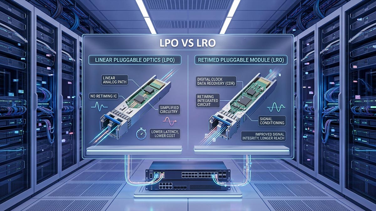
To understand how this new paradigm functions, it is essential to analyze the exact component differences and signal boundaries that separate these emerging technologies. The following breakdown compares the architectural scope, chip placement, and signal paths of Linear Pluggable Optics (LPO) against Linear Receive Optics (LRO).
| Architectural Dimension | Traditional Retimed Optics | Linear Pluggable Optics (LPO) | Linear Receive Optics (LRO) |
| Transmit Path (TX) Component | Full DSP / Retimer included inside the module. | Only a high-linearity driver; no internal DSP or Retimer. | Half-DSP / Retimer retained inside the module for transmission. |
| Receive Path (RX) Component | Full DSP / Retimer included inside the module. | Only a high-linearity Transimpedance Amplifier (TIA). | Only a linear TIA; the internal RX DSP path is entirely removed. |
| Signal Equalization Responsibility | Fully handled inside the transceiver module by the DSP. | Fully shifted to the host ASIC's powerful SerDes. | Split; Host ASIC handles RX equalization, while module DSP handles TX. |
| Primary Design Objective | Maximum interoperability and plug-and-play simplicity. | Absolute minimum module power consumption and ultra-low latency. | A balanced compromise featuring robust TX signal drive with low RX power. |
| Ideal Deployment Distance | Long-reach, multi-kilometer data center interconnects (DCI). | Ultra-short reach, intra-rack AI clusters (< 500m). | Medium-reach, inter-rack or row-to-row connections. |
Why Module Power Dissipation Has Become the Ultimate Data Center Bottleneck
As network architectures transition to high-density 800G and 1.6T configurations, a single network switch can house up to 64 pluggable optical modules. When each traditional module consumes roughly 25W to 30W, the total optical power budget quickly overwhelms the chassis cooling capacity. This massive concentration of heat limits system density, forces expensive cooling upgrades, and lowers overall hardware reliability.
Furthermore, excessive thermal dissipation inside tightly packed line cards creates severe localized hot spots that degrade optical lasers. When lasers run too hot, their lifespan drops drastically, leading to unpredictable network failures and higher maintenance costs. Therefore, reducing module power dissipation is no longer just about cutting electricity bills; it is a strict requirement for system stability.
Key Power Metrics and Efficiency Indicators for Linear and Retimed Modules
To accurately evaluate the performance of these competing optical architectures, engineers track several critical power efficiency indicators. The most prominent metric is the energy-per-bit ratio, typically measured in picojoules per bit (pJ/bit), which quantifies exactly how much energy is spent to move a single bit of data. Lowering this ratio is vital for sustaining the massive throughput required by modern AI workloads.
Another vital metric is thermal density, which measures the heat dissipation per square millimeter of the transceiver's silicon area. Additionally, total system power overhead tracks whether saving power inside the module accidentally triggers an even larger power penalty on the host ASIC SerDes. By analyzing these combined metrics, data center operators can determine whether LPO or LRO offers the best net efficiency.
📖 The Silicon Power Profile of LPO vs LRO: DSP Elimination vs. DSP Splitting
At the heart of the debate between these competing optical architectures lies a fundamental reorganization of the transceiver's silicon layout. The massive power reductions promised by both technologies are achieved by directly altering, reducing, or eliminating the digital signal processing silicon inside the module. Examining these underlying silicon changes reveals the distinct engineering choices that separate true linear operation from a hybrid, split-DSP approach.
Power Consumption of Traditional DSPs in 800G/1.6T Modules
In conventional 800G and emerging 1.6T optical modules, the internal Digital Signal Processor (DSP) operates as a high-performance compute engine. It constantly recalculates and converts complex PAM4 signals to overcome data distortion caused by high-speed fiber transmission. To maintain this level of signal precision, the DSP requires a massive amount of dynamic electrical current.
As data rates double, the power consumption of these traditional silicon chips scales up exponentially rather than linearly. In a standard 800G transceiver, the DSP alone can devour up to 40% to 50% of the entire module's power budget, often pulling nearly 10W on its own. This high power draw creates an immense thermal concentration within a tiny piece of silicon, pushing pluggable modules to their absolute physical limits.
How LPO Achieves Near-Zero Module DSP Power
Linear Pluggable Optics (LPO) resolves this silicon power crisis through a bold engineering choice: completely eliminating the DSP from the transceiver module. Instead of relying on power-hungry silicon chips to retime the signal, LPO modules utilize purely analog, high-linearity drivers and amplifiers. This drastic reduction in component complexity fundamentally changes the electrical landscape inside the pluggable shell.
By removing the digital processing cores, clock recovery circuits, and memory buffers, the module's silicon power profile drops to near-zero levels. The only remaining power draw comes from the low-power analog Transimpedance Amplifiers (TIAs) and laser drivers. As a result, an LPO module operates with incredibly low energy consumption, virtually erasing the traditional thermal footprint of transceiver silicon.
The LRO Compromise: Keeping the TX Retimer While Stripping the RX Path
Linear Receive Optics (LRO) acts as a clever middle ground, choosing to split the traditional DSP architecture rather than completely destroying it. In an LRO configuration, the digital retiming silicon on the receive path (RX) is entirely stripped away, relying on the host system to clean up incoming data. However, a simplified, lower-power retimer or half-DSP is kept intact on the transmit path (TX) to stabilize signals sent to the laser.
This architectural compromise ensures that the optical signal leaving the module meets strict industry standards, making it highly compatible with various network devices. By stripping the RX processing while keeping the TX retimer, LRO cuts the module's silicon power profile by roughly half compared to traditional optics. It provides an elegant fallback solution for network routes where full LPO might struggle with signal degradation.
Comparative Silicon Area and Thermal Dissipation Mechanisms
The physical size of the silicon die inside a module directly determines how much heat it generates and how that heat spreads. Traditional modules require large DSP dies fabricated on advanced, expensive silicon nodes to manage the heavy processing workloads. These large dies concentrate thermal energy into a very small area, creating intense hotspots that are difficult for standard data center cooling systems to alleviate.
In contrast, LPO modules feature much smaller analog silicon footprints, which drastically reduces the surface area generating heat. LRO modules fall right in the middle, utilizing a shrunk, split-DSP die that generates far less localized thermal stress than a full retimer. By reducing or eliminating this heavy silicon area, both LPO and LRO alter the internal thermal dissipation mechanisms, allowing heat to escape smoothly without endangering the internal laser components.
📖 Direct Power Consumption Comparisons: Actual Wattage Profiles of LPO vs LRO
Evaluating the hardware differences between these architectures ultimately leads to a direct comparison of their real-world electricity usage. Examining the actual wattage profiles reveals the true scale of energy reductions when moving away from traditional retimed transceivers. These hard numbers show exactly how much electricity is saved at the plug, at the network switch, and across the entire data center infrastructure.
Per-Port Wattage Metrics for 800G LPO vs LRO Modules
A standard, fully retimed 800G pluggable module typically draws an average of 16 to 20W of power during operation. In comparison, removing the entire DSP allows an 800G LPO module to slash that consumption down to a mere 8 to 10W per port.
Because LRO leaves a partial retimer intact on the transmit side, its power consumption usually hovers around 12 to 14W. This intermediate wattage makes LRO significantly more efficient than traditional modules while using slightly more power than LPO.
Power Savings Calculations at the Switch and Rack Level
When these per-port savings are scaled across a modern 64-port 800G network switch, the cumulative drop in energy consumption is massive. Deploying LPO instead of traditional modules can instantly cut the switch's optical power load by over 600W.
At the server rack level containing multiple high-density switches, these power savings multiply into several kilowatts of saved electricity. This massive reduction dramatically lowers the power delivery requirements for the entire networking layout.
Total Cost of Ownership (TCO) Impact of Reduced Optical Power Budgets
Lowering the required optical power budget directly shrinks operational expenditures by significantly cutting the daily electricity bill. Furthermore, reducing the power draw alleviates the massive thermal load on expensive data center cooling infrastructure.
These combined savings mean that facilities can defer costly upgrades to their power delivery and air conditioning systems. Over a standard multi-year hardware lifecycle, this dramatically lowers the total cost of ownership for high-speed network deployments.
Power Efficiency Profiles Under Maximum Traffic Loads (PAM4 Signaling)
When network traffic peaks, traditional DSPs must work overtime to constantly process dense, complex PAM4 signal matrices. This heavy computational workload causes the power consumption of fully retimed modules to spike unpredictably during peak hours.
Because LPO relies on purely analog amplification, its power profile remains exceptionally flat and stable even under maximum traffic loads. LRO also shows excellent stability, as its stripped-down RX path avoids the massive power surges common to full-scale digital processing.
📖 Signal Integrity Costs of LPO vs LRO: Shifting Power to the Host ASIC
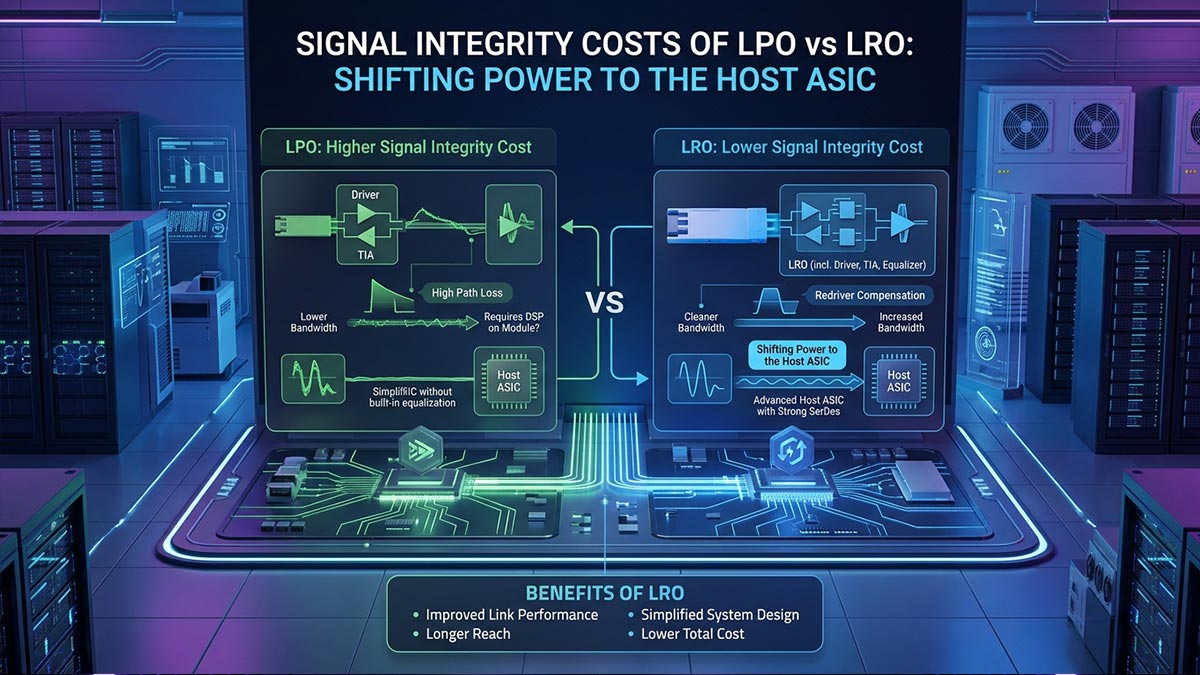
While removing or splitting the module DSP slashes power consumption inside the optical transceiver, that energy savings does not come entirely free. Eliminating the internal retimer forces the host switch ASIC to work much harder to maintain clear, readable data streams. This architectural trade-off shifts the heavy signal compensation workload onto the main board, creating a critical focal point when analyzing the total power shift of LPO vs LRO.
The Burden on Host SerDes Power and Compensation Mechanisms
Without an internal module DSP to clean up data, the host ASIC's SerDes must work overtime to transmit and receive high-speed signals. The host chip must deploy advanced electronic equalization filters to manually repair the distortion caused by the analog optical path.
This heavy processing burden forces the host SerDes to consume significantly more power than it would when paired with traditional retimed optics. Consequently, when evaluating LPO vs LRO, some of the wattage saved inside the pluggable module is simply redirected back into the main switch silicon.
Channel Insertion Loss Budgets and the Resulting Host Compensation Power
High-speed PAM4 signals experience massive signal degradation, or insertion loss, as they travel across the physical circuit boards of the switch. Because LPO eliminates the mid-way retiming step completely, the host ASIC must push enough raw electrical power to overcome the entire link's loss budget.
To compensate for this unshielded channel loss, the host system must run aggressive, power-hungry amplification algorithms. The core difference in LPO vs LRO here is that LRO alleviates some of this physical burden on the transmit side, though it still requires the host to burn extra compensation power on the receive path.
Bit Error Rate (BER) and Forward Error Correction (FEC) Power Overhead
Dropping the dedicated optical retimer naturally causes a slight rise in the raw Bit Error Rate flowing through the high-speed connection. To prevent packet loss, the host system is forced to rely much more heavily on Forward Error Correction (FEC) algorithms to catch and fix data errors.
Running these intense mathematical error-correction processes creates a noticeable digital processing overhead inside the main switch ASIC. In the broader context of LPO vs LRO efficiency, this constant cryptographic computing work draws additional steady-state electricity, partially offsetting the module-level power savings.
Equalization Challenges in Eliminating the Optical Retimer
Completely eliminating the optical retimer means that analog noise and electrical reflections travel unchecked through the entire data path. The lack of a clear digital boundary makes it incredibly difficult for the host ASIC to accurately predict and smooth out signal jitter.
As a result, tuning the system to achieve stable signal integrity requires highly complex, custom firmware settings on the host board. This complex equalization environment remains a primary challenge in the LPO vs LRO debate, often limiting the physical trace lengths allowed between the host ASIC and the optical port.
📖 Processing Power Overheads: How Internal Processing Schemes in LPO vs LRO Impact Total Energy Draw
The specific methods used to handle and synchronize data inside an optical transceiver play a massive role in dictating its overall energy consumption. By contrasting different internal signal processing math and circuitry architectures, operators can see exactly where power is burned or saved. Examining these internal mechanisms provides a clear view of how the engineering choices of LPO vs LRO impact the total system energy draw.
The Power Penalty of Continuous Clock and Data Recovery (CDR) Processing
Traditional optical modules rely on continuous Clock and Data Recovery (CDR) circuits to constantly lock onto, align, and clean up incoming high-speed data streams. This relentless digital synchronization requires active processing cycles that draw a heavy, continuous baseline of electrical current.
The primary operational downsides of keeping full CDR processing active inside a transceiver include:
- High static current: The internal clock phase-locked loops (PLLs) constantly consume energy regardless of data traffic volume.
- Intense thermal output: Continuous mathematical alignment generates a steady stream of localized heat inside the module.
- Increased latency overhead: Regenerating the clock signal adds unavoidable processing delay to the entire data path.
Analyzing the Electrical Power Saved by Bypassing Retiming Steps
Completely or partially bypassing the digital retiming steps allows next-generation architectures to drop heavy data manipulation processes. By removing these complex digital state machines, the transceiver avoids the massive power overhead required to rebuild high-frequency waveforms from scratch.
Eliminating these computational steps from the transceiver yields several immediate electrical advantages:
- Near-zero digital power: Bypassing the retimer reduces the internal digital logic power draw to a negligible level.
- Simplified circuit paths: Removing complex clock networks eliminates the need for power-hungry internal clock distribution trees.
- Direct voltage scaling: The module draws power only for basic analog amplification rather than complex digital calculations.
Asymmetric Power Projections: TX Processing vs. RX Processing Budgets
The energy required to process data is not split evenly between sending and receiving signals across a high-speed optical link. Transmitting data requires precise laser modulation control, while receiving data requires intense noise filtering to fix fiber distortion.
A close look at the asymmetric power budgets highlights the operational differences between the two architectures:
- LPO total minimization: LPO wipes out the digital processing budgets for both the transmit (TX) and receive (RX) pathways inside the module.
- LRO split budget: LRO maintains a digital processing budget for the TX retimer but entirely clears out the RX processing budget.
- Host ASIC shift: Both architectures rely heavily on the host system to shoulder the remaining RX signal restoration workload.
Dynamic Power Scaling of Linear Amplifiers vs. Retimed Signal Conditioners
Traditional retimed signal conditioners run at a fixed, high power consumption rate to keep their digital signal processing cores stable. In contrast, modern analog linear amplifiers feature a much more flexible electrical profile that reacts differently to system changes.
The distinct operational dynamics between these two component types reveal clear differences in energy management:
- Fixed vs. flexible draw: Retimed conditioners consume maximum power continuously, while linear amplifiers maintain a lower, predictable baseline.
- Temperature stability: Linear amplifiers experience minimal power fluctuations when internal line card temperatures rise or fall.
- Signal voltage tracking: Linear components scale their current consumption based strictly on the raw voltage of the incoming electrical waves.
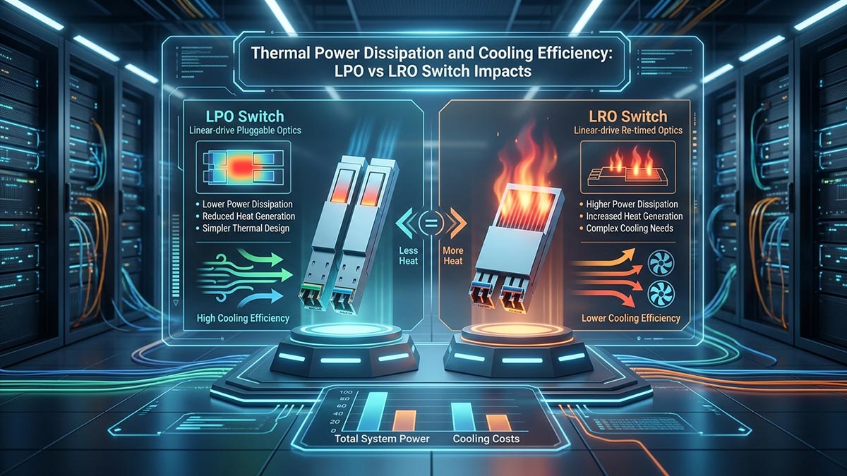
📖 Thermal Power Dissipation and Cooling Efficiency: LPO vs LRO Switch Impacts
Reducing electrical power inside a transceiver module directly translates to a cooler-running network switch chassis. When dealing with high-density hardware layouts, the thermal dissipation characteristics of the chosen optical architecture will dictate the entire cooling strategy of the facility. Evaluating the thermal impacts of LPO vs LRO reveals how significantly these technologies can lower physical strain on data center infrastructure.
Thermal Footprint Reduction in High-Density OSFP/QSFP-DD Line Cards
Modern network line cards pack up to 36 or 64 OSFP/QSFP-DD ports tightly along a single front panel, creating an incredibly dense concentration of heat. Choosing between LPO vs LRO allows operators to drastically alter the localized thermal footprint across these front-row ports.
The primary thermal relief benefits observed at the line card level include:
- LPO absolute minimization: Removing the entire DSP allows LPO to drop cage temperatures to the absolute lowest possible level.
- LRO balanced reduction: Keeping a half-DSP means LRO runs slightly warmer than LPO, but it still eliminates the severe hotspots of traditional modules.
- Even heat distribution: Both architectures allow thermal energy to spread smoothly across the metal cage assembly, preventing dangerous localized heat spikes.
Airflow Requirements and Fan Power Reduction with Linear Optics
When the heat generation inside a network switch drops, the facility can drastically adjust the chassis cooling mechanisms. The choice of LPO vs LRO determines how much active CFM (cubic feet per minute) of forced air is needed to keep the switch safe.
This drop in required airflow leads to several direct mechanical and power advantages:
- Slower chassis fan speeds: Switches loaded with LPO or LRO can run system fans at much lower RPMs during normal operations.
- Exponential fan power savings: Because LPO saves the most module heat, it delivers the deepest cuts to fan electricity consumption.
- Reduced acoustic noise: Lower fan speeds across both architectures result in a much quieter equipment rack environment.
Laser Degradation and Reliability Risks Associated with Module Heat
Optical lasers are highly sensitive to thermal energy, and running them at elevated temperatures accelerates internal degradation. When analyzing LPO vs LRO, managing this internal heat is critical for shielding delicate transmitter lasers from chronic overheating.
The critical long-term reliability improvements achieved by lowering module heat include:
- Extended laser lifespans: LPO provides the coolest environment for the laser diode, while LRO protects the transmitter laser by keeping a stable TX retimer.
- Reduced wavelength drifting: Lower heat across both architectures prevents the optical signal wavelengths from shifting out of specification.
- Higher Mean Time Between Failures (MTBF): Minimizing thermal stress via LPO or LRO drastically lowers unpredictable field failures and maintenance costs.
📖 Final Review: Deciding Between LPO vs LRO for Optimal System Power
Choosing between these two cutting-edge architectures ultimately comes down to balancing raw power savings against your specific signal integrity requirements. While LPO offers the absolute lowest transceiver wattage and latency by removing the DSP completely, LRO provides a highly reliable, plug-and-play compromise by keeping the transmit-side retimer intact. Evaluating your network’s physical trace lengths and host ASIC capabilities will dictate whether LPO or LRO serves as the most efficient path forward for your data center infrastructure.
If you are ready to optimize your high-speed network with high-reliability transceivers and advanced optical components, selecting the right hardware partner is essential. Explore a comprehensive selection of cutting-edge, power-efficient networking solutions by visiting the LINK-PP Official Store to find the ideal modules for your deployment.