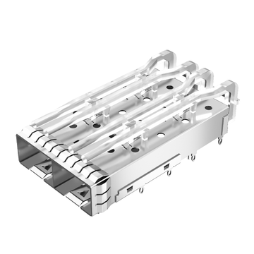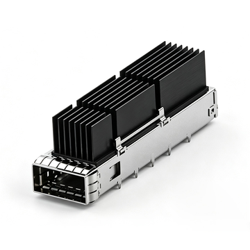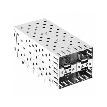
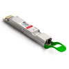
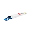
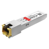
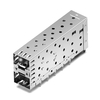
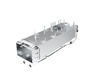
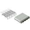

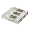

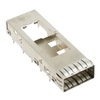
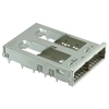
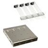




A medida que las redes de alta velocidad evolucionan de 25G NRZ a 112G PAM4 y más allá, ¿cómo pueden los ingenieros de hardware montar un conjunto de módulos multipuerto en placas de circuito impreso densas y multicapa sin comprometer la fiabilidad física de la placa? Las configuraciones SFP, QSFP y OSFP de alta densidad imponen enormes exigencias térmicas y mecánicas a la placa base durante la fabricación. Por consiguiente, elegir el método de terminación adecuado en la capa física se ha convertido en una decisión de ingeniería crítica, más que en una simple preferencia de ensamblaje.
¿Puede la soldadura manual tradicional soportar los estándares modernos de alta frecuencia, o es la tecnología de ajuste a presión compatible la mejor opción para preservar la impedancia de las pistas y reducir la tensión en la PCB? Las temperaturas de soldadura excesivas conllevan el riesgo de deslaminación en el eje Z y de que las vías se deformen, mientras que los pines de ajuste a presión proporcionan estabilidad mecánica sin soldadura y permiten una perforación posterior de precisión. Comprender cómo estas dos técnicas de montaje afectan la tensión en la placa y la integridad de la señal es fundamental para lograr tasas de error de bits óptimas y maximizar el rendimiento de fabricación en plataformas de hardware de alta velocidad.
📋 Introducción al montaje de conjuntos de jaulas ópticas de alta velocidad
El despliegue de interconexiones ópticas en equipos de comunicación modernos exige un equilibrio preciso entre una fijación mecánica rígida y una fidelidad eléctrica a nivel micro. A medida que aumenta el ancho de banda del sistema, el conjunto de la jaula óptica ha evolucionado de una simple carcasa de chapa metálica a un participante activo en la dinámica del canal de la capa física. Por lo tanto, el montaje de estos componentes en placas base congestionadas sin inducir microfisuras ni discontinuidades en el canal se ha convertido en un paso fundamental en la ingeniería de placas.
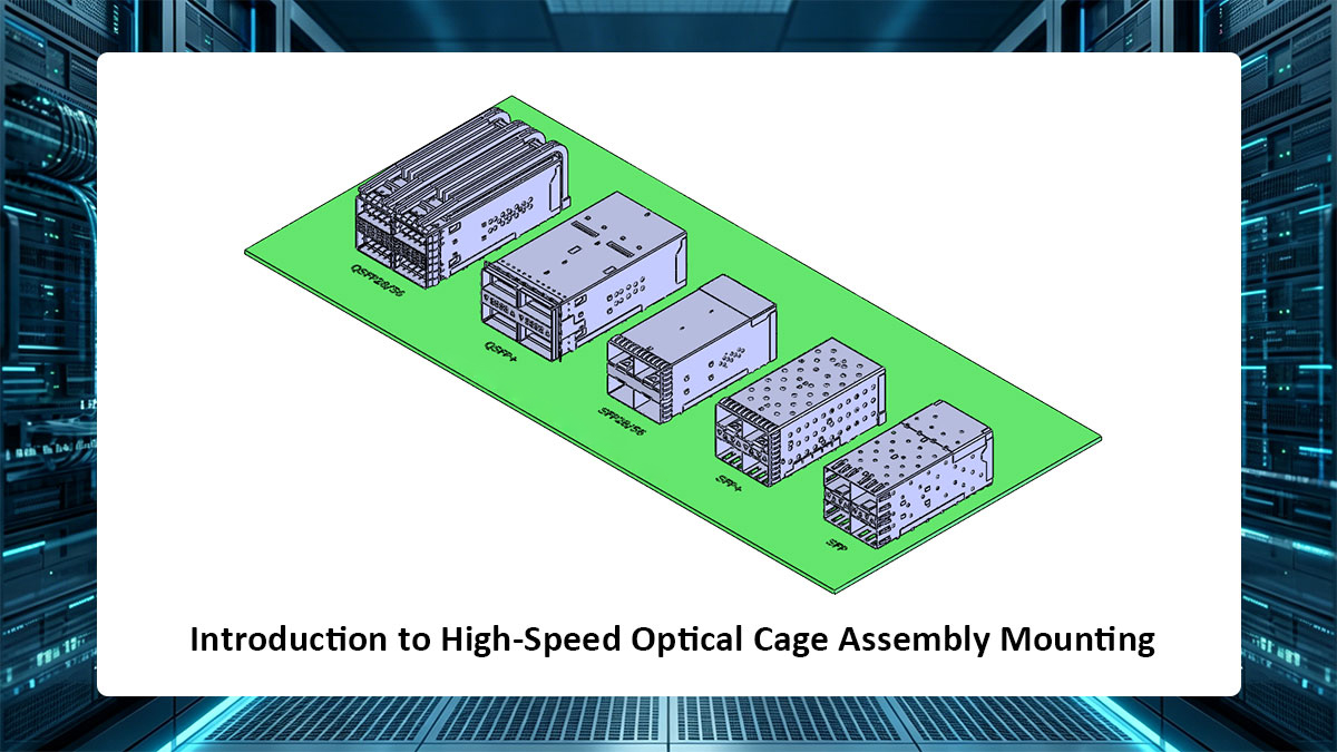
Comprensión de las huellas de ensamblaje de jaulas SFP, QSFP y OSFP
Los factores de forma ópticos varían drásticamente en cuanto a la densidad y las exigencias de disipación térmica en los distintos niveles de red multigigabit:
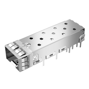
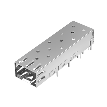
- SFP/SFP+ (de 10G a 28G): Se basa en la señalización de un solo carril, donde los diseños de huella generalmente presentan configuraciones de una sola fila o 1x2 con un menor número total de pines y huellas modestas en la placa.
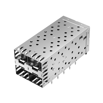
- QSFP28/QSFP-DD (100G a 400G): Las interfaces de cuatro canales, especialmente las configuraciones de unión directa o apiladas de 2x1 y 2x4, aumentan significativamente la densidad de pines, lo que exige una alineación rigurosa de múltiples pines a través de matrices complejas de orificios metalizados pasantes (PTH).
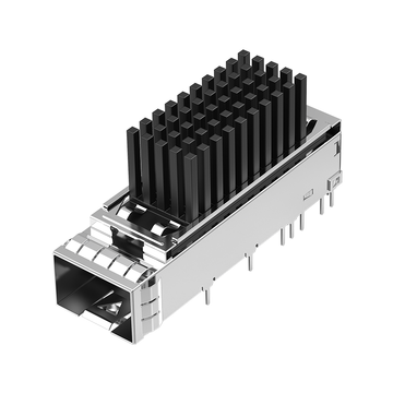
- OSFP (de 400G a 800G): Diseñados para ofrecer el máximo rendimiento térmico y un alto nivel de potencia, los módulos OSFP combinan disipadores de calor integrados de gran tamaño con grupos de pines multicapa extremadamente compactos que amplifican la carga mecánica sobre la placa base.
Debido a que cada generación sucesiva incorpora pasos de contacto más estrechos en la placa de circuito impreso principal, cualquier desalineación en el montaje o inconsistencia física degrada directamente la impedancia del canal.
Compromisos fundamentales en el montaje de PCB y el diseño de capas físicas
La fijación segura de un conjunto de jaula multipuerto implica sortear importantes desafíos físicos y térmicos. Las placas de circuito impreso de 16 a 28 capas actúan como grandes disipadores de calor, lo que requiere un aporte de calor considerable durante la soldadura manual o por ola para humedecer adecuadamente los pines de tierra. Sin embargo, este calentamiento localizado suele provocar grietas en el barril, levantamiento de las almohadillas y deterioro de la resina del sustrato.
Las alternativas de montaje mecánico deben evitar estos graves problemas térmicos sin generar fuerzas de compresión vertical catastróficas. Los diseñadores de hardware deben equilibrar constantemente la resistencia estructural, la resistencia a las vibraciones a largo plazo y el trazado limpio de la placa con la enorme tensión física que se ejerce sobre las delicadas pistas de cobre de la capa interna.
Cómo los estilos de terminación determinan la integridad y la fiabilidad de la señal.
El límite eléctrico donde un pasador de ensamblaje de jaula entra en un orificio pasante metalizado establece directamente la línea base de reflexión inicial del canal:
| Factor de terminación | Interfaz soldada a mano | Interfaz compatible con ajuste a presión |
| Vínculo físico | Puente de soldadura metalúrgico propenso a la formación de huecos y filetes de humectación variables. | Soldadura en frío elástica y hermética mediante fuerza radial mecánica. |
| Continuidad de impedancia | Caídas capacitivas aleatorias causadas por la acumulación y capilaridad desiguales de la soldadura. | Perfil diferencial estable de 100 Ω determinado por la geometría uniforme de los pines. |
| Riesgo de SI a largo plazo | Alta fragilidad de los compuestos intermetálicos (IMC) y propiedades dieléctricas inducidas por fundente. | Alta estabilidad de micromovimientos con cero degradación térmica del barril PTH |
Cuando los métodos de terminación no logran generar una interfaz limpia y uniforme, las señales de alta frecuencia sufren caídas importantes en la pérdida de retorno y fluctuaciones de fase. Elegir el método de terminación adecuado garantiza que la interfaz física proteja el margen del canal en cargas de trabajo exigentes de varios gigabits.
📋 Estrés térmico y mecánico de la placa de circuito impreso durante la instalación del conjunto de la jaula
La transición desde el diseño de la huella hasta el ensamblaje físico revela diferencias notables en las tensiones internas que se imponen a la placa base. Las placas base empresariales, de gran grosor, actúan como disipadores de calor masivos, lo que convierte las operaciones de soldadura a alta temperatura en una amenaza importante para la integridad del laminado. Al sustituir los ciclos térmicos extremos por una inserción mecánica controlada, los métodos de montaje modernos permiten a los ingenieros anclar cada conjunto de jaula, protegiendo al mismo tiempo las estructuras de placas multicapa.

Desajuste del coeficiente de dilatación térmica en el eje Z y riesgos de deslaminación de la placa de circuito impreso
Las tarjetas de red de alta velocidad se basan en laminados densos de múltiples capas, de 16 a 28 capas, que se comportan de forma impredecible bajo cargas térmicas intensas. Al soldar un conjunto de jaula de múltiples pines, el coeficiente de expansión térmica (CTE) del sustrato a lo largo del eje Z vertical se expande mucho más rápido que los cilindros de cobre dentro de los orificios metalizados pasantes (PTH).
Esta grave discrepancia en la expansión induce una tensión mecánica aguda a través de las paredes verticales del orificio, lo que da lugar a varios modos de fallo críticos:
- Agrietamiento en barril: La expansión en el eje Z desgarra el revestimiento de cobre, interrumpiendo la continuidad eléctrica.
- Delaminación de la resina: El calor extremo separa las capas internas de preimpregnado, provocando ampollas en el núcleo del tablero.
- Desprendimiento de las almohadillas: La dilatación térmica desigual provoca el desgarro de los anillos anulares superficiales, separándolos del laminado.
Estos defectos estructurales interrumpen las rutas de enrutamiento de canales de alta velocidad y provocan fallos irreversibles en la placa de circuito impreso.
Riesgos de choque térmico derivados de la soldadura por ola y manual.
Para asegurar las grandes pantallas metálicas y las pestañas de conexión a tierra internas, se requiere una exposición prolongada a altas temperaturas para contrarrestar la rápida disipación del calor en los planos internos de cobre. La soldadura manual obliga a los técnicos a aplicar puntas de soldador calientes directamente sobre los pines durante largos periodos, mientras que la soldadura por ola sumerge toda la parte inferior en soldadura fundida.
Estos ciclos térmicos agresivos someten a los materiales dieléctricos circundantes a un choque térmico inmediato, lo que provoca una grave degradación física:
- Fragilización por resina: Los tiempos de permanencia prolongados degradan las estructuras de transición vítrea alrededor de las vías de alta velocidad.
- Microfisuras: Los fuertes gradientes térmicos agrietan la resina dieléctrica entre las estrechas líneas conductoras.
- Cambios dieléctricos: Los núcleos del sustrato dañados por el calor alteran la permitividad local, modificando la impedancia de la pista.
La eliminación de la soldadura a altas temperaturas evita estas microfracturas localizadas, lo que preserva un rendimiento dieléctrico uniforme en pares diferenciales de alta frecuencia.
Fuerzas de inserción mecánica en jaulas agrupadas con múltiples puertos
El abandono del ensamblaje térmico centra la atención de la ingeniería en la gestión de la fuerza mecánica vertical durante la inserción a presión. Las arquitecturas de alta densidad y múltiples puertos, como las configuraciones apiladas de 2x4 QSFP28 o 2x6 OSFP Cage, albergan cientos de pines compatibles que deben entrar en sus orificios designados simultáneamente.
Debido a que cada pin individual requiere entre 20 N y 40 N de esfuerzo de asentamiento, el asentamiento de un conjunto completo de jaula concentra enormes cargas mecánicas en una superficie reducida de la placa:
- Concentración de carga: Las huellas de múltiples pines generan miles de Newtons de fuerza descendente acumulada.
- Tensión en las pistas internas: Una presión desigual puede aplastar las pistas de cobre de la capa interna que discurren por debajo del conector.
- Compresión dieléctrica: Una fuerza vertical incontrolada distorsiona las capas centrales locales y las altera mediante la simetría.
Gestionar estas intensas cargas de inserción requiere un control mecánico preciso para proteger las vulnerables capas internas de cobre de posibles daños físicos.
Cómo evitar la deformación de la placa durante el prensado de ensamblaje de jaulas pesadas
Aplicar una fuerza de inserción considerable sobre una placa de circuito impreso sin soporte provoca una flexión localizada severa y una deformación permanente del panel. Cuando una placa base se dobla bajo cargas de presión, los orificios metalizados se deforman adquiriendo formas ovaladas, lo que daña la fuerza de retención de los pines y fractura las uniones de soldadura de montaje superficial adyacentes.
Mantener una planitud absoluta de la placa durante el prensado de ensamblaje de jaulas pesadas requiere medidas de seguridad de fabricación específicas:
- Yunques inferiores personalizados: Soportes rígidos que refuerzan la placa directamente debajo del campo de pines del conector.
- Perfilado de fuerza mediante servocontrol: La monitorización en tiempo real de la relación fuerza-distancia detiene la inserción si la resistencia aumenta inesperadamente.
- Sistema de herramientas superiores equilibrado: Los cabezales de prensado mecanizados con precisión aplican una presión descendente perfectamente uniforme en toda la carcasa.
Estos controles de producción eliminan la deflexión localizada de la placa de circuito impreso, manteniendo los orificios pasantes perfectamente cilíndricos y garantizando la integridad de la señal a largo plazo en todos los canales de alta velocidad.
📋 Métricas de integridad de señal de alta frecuencia para la terminación de pines de ensamblaje de jaula
Si bien controlar la deformación de la placa y la presión mecánica la protege físicamente, el método de terminación también determina directamente la calidad de las señales de alta velocidad que se transmiten a través del puerto. En sistemas multigigabit, incluso pequeñas imperfecciones estructurales en la interfaz entre el pin y la placa pueden afectar negativamente el rendimiento del canal. La evaluación de los parámetros clave de integridad de la señal demuestra claramente por qué un ensamblaje de jaula instalado con precisión es fundamental para prevenir errores en la transmisión de datos.

Impacto de la geometría de contacto en el control de la impedancia característica
Para mantener una impedancia diferencial objetivo de 100 ohmios, se requiere una forma limpia y predecible a lo largo de toda la ruta de la señal. La soldadura manual introduce cantidades aleatorias de soldadura, una humectación desigual y soldadura irregular que se introduce en el orificio metalizado.
Estas formas físicas irregulares alteran la capacitancia y la inductancia normales, lo que provoca claras variaciones de impedancia:
- Capacitancia excesiva: Las grandes acumulaciones de soldadura crean caídas capacitivas localizadas muy por debajo de la impedancia objetivo.
- Campos desequilibrados: El flujo irregular de la soldadura distorsiona el límite dieléctrico alrededor de los pares diferenciales.
- Formas de contacto estables: Los pasadores de ajuste a presión flexibles se comprimen uniformemente contra las paredes del orificio, manteniendo tolerancias de impedancia ajustadas y uniformes.
Al eliminar la acumulación aleatoria de soldadura, un conjunto de jaula de ajuste a presión mantiene una geometría de contacto físico uniforme, lo que evita caídas abruptas de impedancia que provocan reflexiones de la señal.
Mitigación de pérdidas de retorno y diafonía en PAM4 de 25G a 112G
A medida que las velocidades de red aumentan de 25G NRZ a 56G y 112G PAM4, los márgenes de ruido más pequeños hacen que los canales sean mucho más sensibles a las reflexiones y al ruido cercano. Las uniones de soldadura no uniformes actúan como puntos de reflexión, lo que empeora la pérdida de retorno y envía energía de vuelta hacia el transmisor.
La propagación impredecible de la soldadura también compromete el blindaje físico entre pares diferenciales adyacentes, lo que aumenta el ruido del canal:
- Mayor pérdida de retorno: Los límites de soldadura discontinuos reflejan la energía de alta frecuencia de vuelta al transceptor de control.
- Mayor diafonía: Los derrames de soldadura alteran las rutas de retorno a tierra, lo que permite que las señales se filtren a los carriles vecinos.
- Bucles de tierra debilitados: La humectación inconsistente de los pines crea un blindaje de tierra deficiente alrededor de las líneas de señal rápidas.
El uso de un conjunto de jaula de ajuste a presión garantiza una separación simétrica entre los pines y la tierra, manteniendo los canales de alta densidad bien aislados y minimizando la diafonía.
Degradación de la pérdida de inserción causada por residuos de soldadura e IMC
La soldadura introduce subproductos químicos y metálicos que aumentan directamente la pérdida de señal. El calor de la soldadura crea compuestos intermetálicos (IMC) frágiles en la interfaz de cobre, que son mucho más resistivos que el pin de cobre original.
Los fundentes de soldadura estándar también dejan residuos químicos en el campo de pines del conector:
- Contaminación dieléctrica: Los residuos de fundente atrapados alteran las propiedades eléctricas de la superficie de la placa, aumentando la atenuación de la señal.
- Pérdidas en el conductor: Las capas de aleación frágiles aumentan la resistencia en los puntos donde las señales de alta frecuencia viajan a lo largo de la superficie del conductor.
- Interfaces limpias: Las conexiones de compresión en frío sin soldadura no generan residuos químicos, dejando intacto el laminado de la placa.
Evitar el calor de la soldadura garantiza que la terminación del conjunto de la jaula mantenga bajas las pérdidas del conductor y preserve los materiales base de la placa de circuito impreso.
Claridad del diagrama de ojo y verificación de la tasa de error de bits (BER)
El impacto combinado de las caídas de impedancia, la diafonía y las pérdidas adicionales se evidencia claramente en las mediciones del diagrama de ojo del receptor. Debido a que PAM4 divide las amplitudes de la señal en múltiples pasos más pequeños, las alturas del ojo son mucho menores y, por lo tanto, mucho más propensas a distorsionarse que las señales NRZ más antiguas.
Cuando la terminación de pines introduce inconsistencia física y fluctuación, el diagrama de ojo de la señal se cierra rápidamente, lo que aumenta las tasas de error de bits:
- Reducción de la altura del diagrama de ojo: Las caídas de impedancia comprimen las aberturas verticales del diagrama de ojo, reduciendo el margen de voltaje vital en el receptor.
- Mayor fluctuación: Las diferencias de fase debidas a uniones de pasadores irregulares amplían la fluctuación horizontal, reduciendo la ventana de muestreo.
- Altas tasas de error de bits: Los ojos cerrados sobrecargan los chips de corrección de errores, lo que provoca la pérdida de paquetes y fallos en el entrenamiento del enlace.
La instalación de un conjunto de jaula de ajuste a presión preserva las amplias aberturas para los ojos, lo que garantiza que los transceptores modernos alcancen sus tasas de error de bits objetivo de forma consistente durante las pruebas de conformidad de alta velocidad.
📋 Mediante la eliminación de salientes y la perforación posterior en el diseño del ensamblaje de la jaula.
Incluso con un control estricto de la impedancia y una tensión reducida en la placa, el rendimiento del canal puede verse afectado negativamente si se descuida la geometría de los orificios pasantes verticales. En placas multicapa gruesas, la parte no utilizada de un orificio pasante metalizado actúa como una ramificación eléctrica abierta que distorsiona gravemente las señales de alta frecuencia. Evaluar cómo interactúa el montaje de los pines con la perforación posterior revela por qué seleccionar el método de terminación adecuado para cada conjunto de jaula es esencial para eliminar las reflexiones parásitas destructivas.
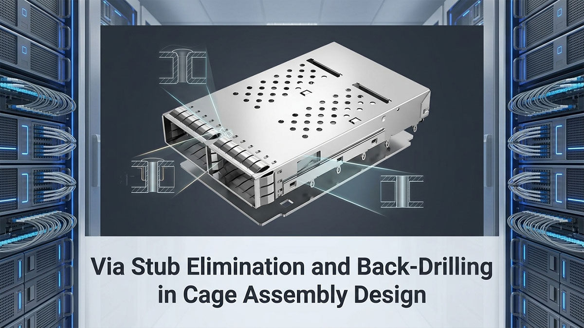
La penalización por resonancia de los segmentos pasantes metalizados no utilizados
Cuando una señal de alta velocidad pasa de una capa superior de PCB a un pin de ensamblaje de jaula, cualquier remanente de cobre debajo de la capa de enrutamiento forma un segmento de vía eléctrica. Este remanente no utilizado se comporta como una línea de transmisión abierta, reflejando la energía de vuelta al canal activo desfasada. Las ondas estacionarias resultantes crean profundas muescas de atenuación que destruyen los márgenes del canal y provocan una pérdida de paquetes impredecible.
A medida que aumenta la velocidad de la señal, incluso un stub de vía microscópico genera suficiente carga capacitiva como para perjudicar la transmisión de alta frecuencia. En enlaces multigigabit, eliminar estos stubs resonantes no deseados es tan crucial como enrutar pares diferenciales limpios a través de la placa principal.
Cómo el ajuste a presión con pasador flexible permite una perforación posterior de precisión
La tecnología de ajuste a presión es inherentemente compatible con el taladrado posterior automatizado con control de profundidad durante la fabricación de la placa. Los fabricantes de PCB pueden taladrar el barril de cobre no utilizado de la parte posterior de la placa antes del montaje de los componentes, dejando solo la longitud de contacto mínima necesaria para sujetar el pin compatible. Dado que el orificio queda libre de material de relleno, la longitud restante del vástago puede mantenerse muy por debajo de 0.2 mm.
Cuando se inserta posteriormente un conjunto de jaula de ajuste a presión en la placa, su pasador flexible se asienta de forma segura en el barril superior activo sin alterar la cavidad libre que se encuentra debajo. Esta separación mecánica precisa permite a los diseñadores de hardware eliminar por completo las vías de conexión, manteniendo al mismo tiempo una excelente fuerza de retención mecánica.
Fallos en la absorción de la soldadura que impiden la extracción de los extremos soldados en jaulas.
Intentar controlar las conexiones mediante salientes en placas soldadas a mano o por ola presenta serios obstáculos de fabricación. La soldadura asciende y llena los orificios metalizados por capilaridad, tapando por completo cualquier cavidad que debería haber quedado libre. Una vez que la soldadura fundida fluye por un orificio sin perforar o inunda un orificio perforado en la parte posterior, recrea permanentemente el saliente eléctrico hasta la capa inferior.
Intentar taladrar un orificio después de soldar es prácticamente imposible, ya que las brocas estándar se desvían o se rompen al chocar con la soldadura y los pines endurecidos. En consecuencia, un conjunto de jaula soldada deja a los ingenieros de hardware con vías incontrolables, atrapando permanentemente las reflexiones de la señal dentro de la placa base.
Efectos de resonancia de un cuarto de longitud de onda a 28 GHz y 56 GHz Nyquist
A velocidades de línea propias de las interfaces PAM4 de 56G y 112G, las frecuencias fundamentales de Nyquist se sitúan en 28 GHz y 56 GHz, respectivamente, donde las longitudes de onda físicas se reducen drásticamente. Un segmento de vía de tan solo 0.5 mm se convierte en un resonador de un cuarto de longitud de onda a estas frecuencias, lo que provoca una caída masiva en la transmisión de la señal en toda la banda de operación. Esta severa atenuación por resonancia anula por completo la amplitud de la señal y cierra el diagrama de ojo del receptor.
El uso de un conjunto de jaula de ajuste a presión es la única forma fiable de mantener los segmentos residuales lo suficientemente cortos como para desplazar la frecuencia de resonancia de un cuarto de longitud de onda fuera del canal de operación de forma segura. Eliminar esta muesca de alta frecuencia garantiza bandas de transmisión uniformes, baja pérdida de retorno y una transmisión de datos fiable en el hardware de red de última generación.
📋 Dinámica de pasadores elásticos y flexibles en la integración de ensamblajes de jaulas de ajuste a presión
Para comprender cómo la tecnología de ajuste a presión supera la resonancia de los segmentos, es necesario analizar con detalle la conexión mecánica dentro del orificio metalizado. En lugar de depender del calor o de soldaduras frágiles, los pines de ajuste a presión flexibles utilizan la energía elástica almacenada para establecer una vía eléctrica estable y de baja resistencia. El estudio de la mecánica física de esta interfaz con resorte muestra cómo cada conjunto de jaula mantiene la integridad estructural de la placa y un rendimiento óptimo a altas frecuencias durante años de uso continuo.

Principios mecánicos del pasador flexible de ojo de aguja
El pasador "Eye-of-the-Needle" (EON) cuenta con una abertura central estampada con precisión, flanqueada por vigas elásticas exteriores flexibles. A medida que el pasador entra en un orificio pasante metalizado ligeramente más pequeño, estas vigas se comprimen hacia adentro, convirtiendo el esfuerzo de inserción vertical en una fuerza radial continua hacia afuera contra la pared de cobre del orificio.
- Deformación elástica controlada: Las vigas de resorte curvas absorben la mayor parte de la tensión de inserción, evitando así el desgaste físico pronunciado contra el interior del orificio.
- Precarga radial continua: La fuerza del resorte almacenada mantiene el pin firmemente asentado contra la pared del orificio pasante, incluso cuando la placa se expande y contrae debido a las variaciones de la temperatura ambiente de funcionamiento.
- Geometría exterior equilibrada: La presión uniforme hacia afuera evita la ovalización del barril del orificio, manteniendo los pares de pines diferenciales alineados simétricamente en la placa de circuito impreso principal.
Al basarse en la deflexión predecible del haz en lugar del prensado rígido, un conjunto de jaula de ajuste a presión protege las delicadas láminas de cobre de la capa interna de fracturas mecánicas durante la instalación.
Interfaces de soldadura en frío herméticas a los gases sin daños térmicos.
Cuando un pasador flexible se inserta en un orificio metalizado, la alta presión de contacto empuja el revestimiento exterior del pasador directamente contra la capa de estaño u oro de la vía. Esta intensa presión localizada provoca que las crestas microscópicas de la superficie se deformen plásticamente, creando una interfaz de soldadura en frío hermética al aire y a los gases a temperatura ambiente.
Debido a que este sellado físico se forma completamente sin calor de soldadura, proporciona importantes beneficios estructurales y eléctricos en todo el campo de pines del conector:
| Parámetro físico | Sello hermético a presión | Junta soldada convencional |
| Protección contra la oxidación | Bloquea la entrada de aire corrosivo y humedad en el límite de contacto. | Los residuos de fundente y los huecos en la superficie permiten la formación de microcanales corrosivos. |
| Resistencia de contacto | Mantiene una resistencia ultrabaja y submiliohm durante largos periodos de funcionamiento. | Aumenta con el tiempo a medida que se expanden las microfisuras del compuesto intermetálico (IMC). |
| Deformación térmica | Ausencia de tensión de expansión térmica impuesta al núcleo de PCB multicapa | Un choque térmico localizado severo conlleva el riesgo de ampollas en los preimpregnados de resina internos. |
Esta barrera de aplicación en frío sella los gases industriales corrosivos, manteniéndolos alejados de la ruta de la señal activa y asegurando que el conjunto de la jaula mantenga una conductividad eléctrica impecable sin riesgo de daños térmicos en la placa.
Tolerancias y reglas de recubrimiento para orificios pasantes metalizados (PTH) en placas de circuito impreso (PCB).
Para lograr una retención fiable y conforme a las normas, protegiendo al mismo tiempo las capas internas de cobre, es fundamental cumplir estrictamente con las dimensiones de los orificios de la placa de circuito impreso y las especificaciones de recubrimiento superficial. Si las dimensiones finales de los orificios se desvían de las tolerancias recomendadas, la fuerza de contacto resultante no logrará sujetar el pin de forma segura o bien provocará una rotura permanente en el orificio pasante.
Las directrices de fabricación para la integración conforme de los pines se centran en un control estricto de la perforación y el recubrimiento:
- Tolerancias de perforación a acabado: Los diámetros de los orificios terminados deben mantener una tolerancia estricta de aproximadamente ±0.05 mm en toda la superficie del conector.
- Espesor del barril de cobre: El cobre electrodepositado en el interior de la pared del orificio pasante debe tener un espesor promedio de al menos 25 μm (1 mil) para evitar roturas en el recubrimiento durante la colocación de los pines.
- Selección del acabado superficial: El estaño por inmersión (ImSn) o el níquel químico con recubrimiento de oro por inmersión (ENIG) proporcionan interfaces de asiento planas y lubricadas que evitan el desgarro del cobre.
Seguir estas reglas de recubrimiento precisas garantiza que cada pin del conjunto de la jaula entre sin problemas, manteniendo las capas dieléctricas circundantes planas e intactas.
Resistencia a largo plazo a golpes y vibraciones durante ciclos térmicos
Los entornos operativos de los centros de datos de alta densidad someten a las placas base a vibraciones mecánicas continuas de los ventiladores y a ciclos térmicos fluctuantes. Las uniones soldadas a mano tienden a endurecerse y a desarrollar microfisuras bajo cambios repetidos de temperatura debido a las diferencias en los coeficientes de expansión entre las aleaciones de soldadura y los laminados de la placa.
Los pasadores flexibles actúan como amortiguadores en miniatura que neutralizan activamente la fatiga estructural:
- Compensación dinámica del coeficiente de dilatación térmica: Las vigas de resorte flexibles se flexionan dinámicamente, absorbiendo la expansión diferencial entre la carcasa del conector y el laminado base.
- Inmunidad a la fatiga de la soldadura: Al carecer de capas límite intermetálicas frágiles, la unión no puede desarrollar fracturas por fatiga bajo la turbulencia de un ventilador de alta frecuencia.
- Retención estable del módulo: La elevada fuerza de retención residual evita que el conector se salga de la placa durante los ciclos repetidos de acoplamiento del módulo óptico.
Esta resistencia mecánica garantiza que el conjunto de la jaula de ajuste a presión permanezca firmemente anclado e intacto, evitando pérdidas intermitentes de paquetes y preservando los márgenes del canal físico durante periodos de uso exigentes que se extienden por varios años.
📋 Rendimiento de fabricación, inspección y retrabajo para puertos de ensamblaje de jaulas
Si bien la correcta mecánica de los pines garantiza un rendimiento operativo fiable, la rentabilidad real de la fábrica depende en gran medida de la consistencia del ensamblaje y de la seguridad en la reparación de la placa. La técnica de montaje elegida determina directamente si las placas base de conmutadores de alta densidad superan las pruebas finales de fábrica o sufren costosos daños físicos durante la fabricación.

Uniones de soldadura frías y microvacíos en almohadillas de soldadura densas
Los conectores multipuerto soldados de alta densidad actúan como enormes disipadores de calor, extrayendo rápidamente el calor de las puntas de los soldadores. Esta rápida disipación del calor suele provocar una humectación incompleta de la soldadura, creando uniones frías ocultas y microcavidades de aire en el interior de los orificios metalizados.
Debido a que la carcasa metálica sólida bloquea por completo la visión del campo de pines, la inspección visual estándar y la inspección óptica automatizada no pueden verificar la calidad de la unión. Estos huecos ocultos interrumpen el flujo de corriente y provocan desajustes de impedancia intermitentes, lo que requiere costosas inspecciones por rayos X para su detección.
Herramientas, soporte de fijación inferior y monitorización de la prensa servoaccionada
El montaje de una jaula de ajuste a presión convierte el ensamblaje en un proceso mecánico automatizado y altamente repetible. Los soportes inferiores rígidos sostienen la placa directamente debajo del campo de pines, evitando que se flexione y manteniendo los orificios pasantes perfectamente alineados.
Las prensas servo automatizadas miden la fuerza de inserción y la profundidad de asentamiento en tiempo real durante toda la carrera de prensado. Si la máquina detecta una resistencia anormal debido a un pasador desalineado o un tamaño de orificio incorrecto, se detiene inmediatamente, evitando así tensiones ocultas en la placa y preservando el trazado de los canales.
Procedimientos seguros de extracción en campo y reprensado multiciclo
Los pines del conector o las carcasas de los puertos a veces sufren daños físicos durante las pruebas o la instalación del transceptor, lo que requiere el reemplazo del conector. Las herramientas de extracción mecánicas específicas sujetan el conjunto de la jaula de ajuste a presión y lo extraen hacia arriba, retirando la unidad sin aplicar calor a la placa base.
Gracias a la flexibilidad de los pines, los orificios pasantes metalizados conservan su superficie lisa y su integridad estructural tras su extracción. Los técnicos pueden insertar un conector de repuesto en los mismos orificios hasta dos o tres veces, restaurando por completo la integridad de la señal sin comprometer la fiabilidad de la placa.
Riesgos de desoldadura destructiva en placas multicapa de alta densidad
Retirar un conector multipuerto soldado de una placa gruesa de 16 a 28 capas es una tarea de alto riesgo y, a menudo, destructiva. Los técnicos deben aplicar aire caliente intenso sobre docenas de pines de tierra durante largos periodos para fundir simultáneamente las soldaduras.
El calor prolongado que genera este proceso de retrabajo suele provocar el levantamiento de las almohadillas superficiales, el agrietamiento del cobre de la capa interna y una grave delaminación de las placas de circuito impreso. En hardware de red de alta densidad, intentar desoldar un conector dañado casi siempre destruye los componentes de paso fino cercanos y arruina toda la placa base.
📋 Guía de selección basada en la aplicación para LINK-PP Herrajes para el ensamblaje de la jaula
En última instancia, equilibrar el rendimiento de fabricación con el rendimiento de alta frecuencia guía a los arquitectos de hardware a la hora de evaluar entornos operativos reales. Seleccionar entre los estilos de terminación por presión y soldadura requiere asignar directamente las exigencias específicas de velocidad de datos y las limitaciones físicas del chasis al hardware de conector adecuado.

Conmutadores de nube a hiperescala e implementaciones Spine-Leaf de 400G/800G
Los centros de datos a escala de nube dependen de conmutadores ultradensos de 400G y 800G que ejecutan señalización PAM4 de 56G o 112G por carril a través de planos posteriores multicapa gruesos. En estos conmutadores de tejido masivos, el despliegue de un ajuste a presión de alta densidad LINK-PP El ensamblaje de la jaula es esencial para soportar la perforación posterior de precisión y eliminar los ramales pasantes parásitos.
La arquitectura de pines sin soldadura protege las costosas placas base de 24 capas de la deslaminación térmica destructiva en el eje Z durante la producción. Además, la geometría de pines estrictamente controlada mantiene curvas de impedancia diferencial de 100 Ω limpias y diagramas de ojo de receptor abiertos, lo que garantiza que las plataformas de rack alcancen objetivos estrictos de tasa de error de bits bajo cargas de red elevadas.
Routers de borde reforzados y sistemas de automatización industrial
Los conmutadores de borde industriales están sometidos a fuertes vibraciones de maquinaria, intensos impactos por caída y amplios rangos de temperatura de funcionamiento. Los ensamblajes de jaula soldados a mano o mediante soldadura por ola solo son viables en placas de baja velocidad (inferiores a 10 Gbps, como las SFP/RJ45 de 1 Gbps) y de pocas capas (normalmente menos de 8 capas), donde los grandes filetes de soldadura proporcionan una gran resistencia mecánica al corte y la tensión de expansión térmica se mantiene mínima.
Cuando el enrutamiento de borde industrial alcanza velocidades de 25G o 100G, las uniones soldadas quedan completamente descartadas debido a la presencia de vías no controladas y fallos por pérdida de retorno de alta frecuencia. Para estos enlaces ascendentes robustos de alta velocidad, el estándar de la industria consiste en utilizar un conjunto de jaula de ajuste a presión con tornillos de fijación integrados. Esta arquitectura híbrida proporciona la robustez necesaria para resistir golpes y vibraciones, mientras que los pines flexibles protegen las rutas de señal de alta velocidad de las caídas de impedancia.
Plataformas Open RAN para fronthaul y centrales telefónicas 5G
Las estaciones base 5G, las unidades de radio remotas (RRU) y las plataformas RAN abiertas requieren conexiones ópticas exteriores fiables que operen bajo amplias fluctuaciones de temperatura ambiente. Las carcasas exteriores montadas en postes están expuestas a ciclos térmicos rápidos que someten a tensión el límite físico entre los pines del conector y los orificios metalizados.
Adoptar un ajuste a presión conforme LINK-PP El ensamblaje de la jaula elimina las uniones de soldadura frágiles que se agrietan con el paso de los años debido a la expansión y contracción térmica. La soldadura en frío hermética, formada por pines elásticos y flexibles, protege las rutas de señal activas de la humedad ambiental y los contaminantes corrosivos, lo que garantiza enlaces de comunicación CPRI y eCPRI de fronthaul ininterrumpidos en implementaciones de telecomunicaciones exigentes.
📋 Veredicto final: Mejores prácticas para LINK-PP Terminación del conjunto de jaula óptica

Para hardware de alta velocidad de 25G a 800G, la terminación por ajuste a presión ofrece una tensión en la PCB significativamente menor y una integridad de señal superior en comparación con la soldadura manual. La eliminación de altas cargas térmicas previene la delaminación a nivel de placa, mientras que los pines flexibles sin soldadura permiten una perforación posterior de precisión para eliminar las resonancias de alta frecuencia de los stubs de vía. Para sistemas de alta densidad, el montaje flexible ofrece una fiabilidad física inigualable y líneas de transmisión de 100Ω consistentes.
Para maximizar la integridad de la señal y evitar daños en la placa durante la producción, los ingenieros de hardware deben seguir estas prácticas de implementación esenciales:
- Aplique tolerancias estrictas para los orificios pasantes chapados: Mantenga los diámetros de las brocas pasantes chapadas dentro de ±0.05 mm con acabados de estaño por inmersión o ENIG para garantizar un asentamiento de pasadores hermético a los gases.
- Implemente un sistema de fijación específico: combine siempre las jaulas multipuerto con yunques de fondo plano y prensas servoaccionadas para evitar la flexión localizada de la placa durante la inserción.
- Aislamiento de vías no utilizadas: combine perfiles de pines de ajuste a presión con perforación posterior automatizada para eliminar las muescas de resonancia en las bandas de Nyquist PAM4 de 56 GHz.
- Uso obligatorio de kits de extracción controlada: Utilice herramientas de extracción vertical aprobadas por el fabricante durante la reparación de puertos para preservar las capas internas de cobre y garantizar un prensado seguro en múltiples ciclos.
¿Está diseñando conmutadores de centro de datos de próxima generación, plataformas de banda base 5G o hardware de borde de alta velocidad? Visite el LINK-PP Tienda Oficial Consulte nuestra gama completa de opciones de ensamblaje de jaulas SFP, QSFP y OSFP, diseñadas para obtener señales nítidas y un montaje sencillo en la placa de circuito impreso.