The SFP form factor has become a foundational standard in modern optical and networking equipment, enabling flexible, hot-swappable connectivity across a wide range of applications. As network demands continue to grow, understanding how SFP modules operate beyond their physical interface — especially at the data and control level — has become increasingly important. Central to this is the SFF-8472 specification, which defines the structure and access to digital diagnostics and device information within SFP modules.
At the core of the SFP form factor lies an I2C-based memory architecture that allows systems to communicate with the module in a standardized way. Through defined memory maps and registers, network devices can retrieve critical information such as vendor details, operating conditions, and real-time performance metrics. This article explores how the SFP memory map is organized, how registers function, and why this structure is essential for monitoring, management, and reliable operation of optical modules.
? Overview of SFP Form Factor and SFF-8472 Standard
The SFP form factor defines a compact, hot-pluggable interface widely used in optical and copper networking applications. To enable interoperability and intelligent monitoring, the SFF-8472 standard extends SFP capabilities by defining a digital diagnostics interface. Together, they form the foundation for standardized communication, identification, and performance monitoring in modern transceivers.
What is SFP (Small Form-factor Pluggable)
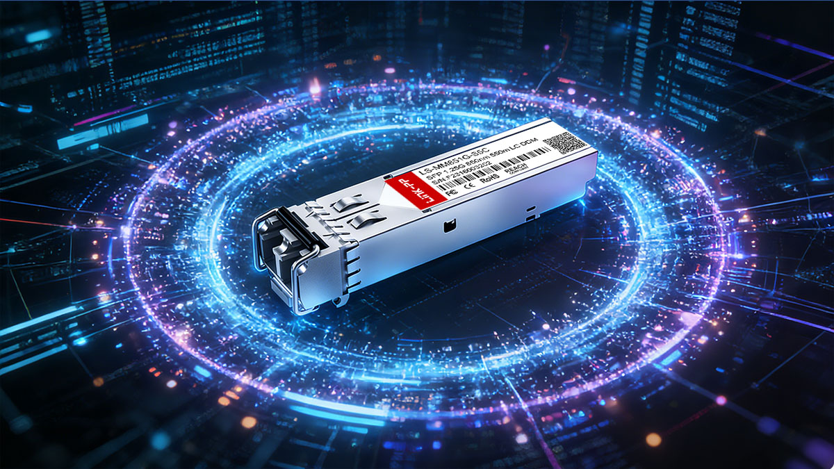
SFP (Small Form-factor Pluggable) is a compact, modular optical transceiver used in networking devices such as switches, routers, and network interface cards. It supports both optical fiber and copper connections, allowing flexible deployment across different transmission media and distances.
The key advantage of the SFP form factor is its hot-pluggable design, which enables modules to be inserted or removed without powering down the system. This improves maintenance efficiency and scalability. SFP transceiver modules also support a wide range of data rates and protocols, making them suitable for Ethernet, Fibre channel, and other communication standards.
Introduction to SFF-8472 Specification
The SFF-8472 specification is an industry standard that defines the digital diagnostic monitoring (DDM) interface for SFP modules. It specifies how internal parameters — such as temperature, voltage, optical power, and bias current — are measured, stored, and accessed via a standardized I2C interface.
In addition to real-time diagnostics, SFF-8472 also defines a memory map structure that includes static information like vendor details, part numbers, and compliance codes. This allows host systems to both identify the module and monitor its operational status in a consistent way.
To better understand its structure, the key elements defined by SFF-8472 are summarized below:
| Feature |
Description |
| I2C Interface |
Standard two-wire serial interface for communication. |
| Memory Map (A0h & A2h) |
Defines address spaces for ID and diagnostic data. |
| Digital Diagnostics (DDM) |
Enables real-time monitoring of module parameters. |
| Calibration Support |
Provides scaling factors for accurate measurement readings. |
| Alarm & Warning Flags |
Indicates abnormal operating conditions. |
| Compatibility |
Ensures interoperability across vendors and platforms. |
Relationship Between SFP Modules and I2C Interface
The SFP form factor relies on an I2C (Inter-Integrated Circuit) interface as the primary communication channel between the host device and the module. This two-wire interface — consisting of a data line (SDA) and a clock line (SCL) — allows the host to read from and write to the module’s internal EEPROM.
Through the I2C interface, the host system can access both static information (such as vendor name and serial number) and dynamic diagnostic data. The use of a standardized protocol ensures consistent communication behavior across different SFP vendors and implementations.
Why Memory Mapping Matters in SFP Modules
Memory mapping is a critical concept in the SFP form factor because it organizes how data is stored and accessed within the module. By defining fixed byte locations for specific parameters, the SFF-8472 standard ensures that host systems can reliably retrieve information without ambiguity.
This structured approach enables efficient monitoring, troubleshooting, and automation. For example, network management systems can quickly read temperature or optical power values from predefined addresses, allowing real-time health checks and predictive maintenance. Without standardized memory mapping, interoperability and diagnostics would be significantly more complex.
? SFP Form Factor Hardware Interface and I2C Communication
The SFP form factor combines a standardized physical interface with a simple yet powerful communication mechanism based on the I2C protocol. This combination enables seamless interaction between the host system and the transceiver module. To access module data and ensure reliable operation, it is essential to understand both the hardware interface and I2C communication.
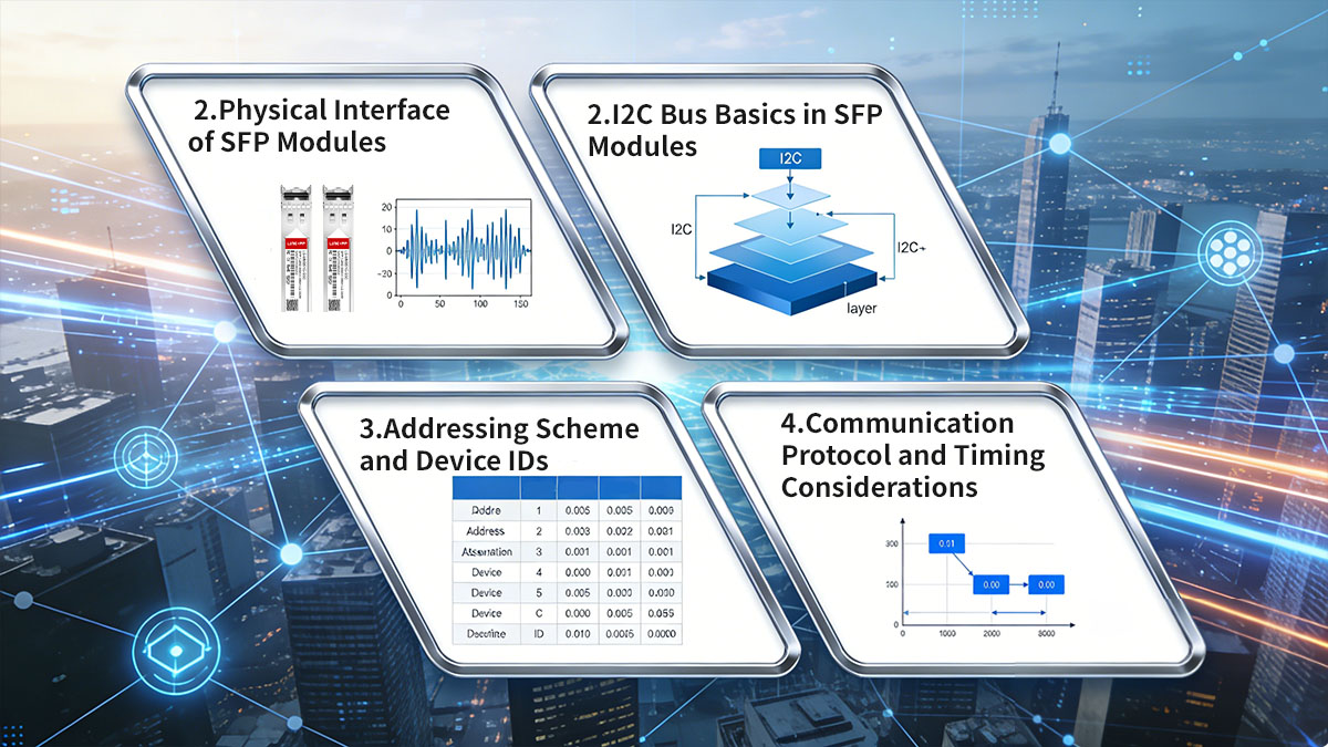
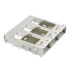
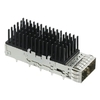
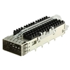
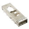
Physical Interface of SFP Modules
The physical interface of SFP modules is defined by a compact, hot-pluggable design that ensures compatibility across networking equipment. Each module connects to the host through a 20-pin edge connector, which carries power, high-speed data signals, and control lines. This standardized form factor allows modules from different vendors to be used interchangeably.
In addition to the main data paths, several control and status pins play an important role in module operation. For example, TX_DISABLE is used to turn off the transmitter, TX_FAULT indicates a failure condition, and RX_LOS signals loss of incoming optical power. The MOD_DEF pins are particularly important, as they are used for module detection and provide access to the I2C communication interface. These hardware signals ensure that the host can both control and monitor the module effectively.
I2C Bus Basics in SFP Modules
The SFP form factor uses a simple two-wire I2C bus to enable communication between the host and the module. This interface consists of a serial data line (SDA) and a serial clock line (SCL), both of which are managed by the host device acting as the master.
Through this bus, the host can read from and write to the module’s internal EEPROM, accessing information such as identification data and real-time diagnostics. The communication operates at relatively low speeds compared to data transmission, but it is sufficient for monitoring and control purposes. Because I2C is a widely adopted standard, it ensures consistent behavior and easy integration across different systems.
Addressing Scheme and Device IDs
SFP modules follow a fixed and standardized I2C addressing scheme defined by SFF-8472. Two primary device addresses are used: A0h (0x50) for static identification data and A2h (0x51) for dynamic diagnostic information. This separation allows the host system to clearly distinguish between different types of data stored within the module.
The addressing follows the standard 7-bit I2C format, ensuring compatibility with common controllers. In some cases, extended memory access is supported through page selection mechanisms, allowing access to additional data beyond the base address space. Overall, this structured addressing approach simplifies communication and improves interoperability.
Communication Protocol and Timing Considerations
Communication over the I2C interface follows a well-defined protocol that ensures reliable data transfer. Each transaction begins with a START condition and ends with a STOP condition, with data transmitted in byte-sized units followed by acknowledgment bits.
To maintain stable communication, several timing considerations must be observed:
- The host controls the clock signal, but the module may use clock stretching if it needs more time to respond.
- Proper setup and hold times must be maintained according to I2C specifications.
- Pull-up resistors are required on both SDA and SCL lines to ensure signal integrity.
- The bus speed should remain within supported limits (typically standard mode).
Failure to meet these timing requirements can lead to communication errors such as missing acknowledgments or bus timeouts. Therefore, careful design and adherence to the protocol are essential for reliable operation of the SFP form factor interface.
? SFP Form Factor Memory Map Structure Explained
The SFP form factor uses a standardized memory map defined by the SFF-8472 specification to organize both static and dynamic data within the module. This structure enables the host system to access information in a predictable and efficient way. Correctly interpreting module data and implementing reliable monitoring both depend directly on the memory structure.

Overview of the 256-Byte Address Space
At the core of the SFP memory architecture is a 256-byte address space accessible via the I2C interface. This address space is divided into blocks that store different types of information, including identification data and diagnostic parameters.
Each byte within this space has a predefined meaning according to the SFF-8472 standard. This fixed mapping allows the host system to directly read specific parameters — such as vendor name or temperature — by accessing known byte offsets. The structured layout eliminates ambiguity and ensures consistent interpretation across different SFP modules.
Lower Memory (A0h) vs Upper Memory (A2h)
The SFP memory map is logically divided into two main regions: lower memory (A0h) and upper memory (A2h). Each region serves a distinct purpose and is accessed through different I2C device addresses.
Lower memory (A0h) primarily contains static identification information that does not change during operation, while upper memory (A2h) stores dynamic diagnostic data and control-related information. This separation helps optimize access patterns and simplifies data management.
The key differences between these two memory regions are summarized below:
| Memory Area |
I2C Address |
Content Type |
Description |
| Lower Memory |
A0h (0x50) |
Static (Read-Only) |
Vendor info, part number, compliance codes |
| Upper Memory |
A2h (0x51) |
Dynamic (Read/Write) |
Diagnostics, alarms, calibration data |
Page Selection Mechanism
In addition to the base 256-byte address space, some SFP modules support extended memory through a page selection mechanism. This allows access to additional data beyond the standard address range without changing the I2C device address.
Page selection is typically controlled by writing to a specific byte in the memory map, which acts as a page pointer. Once a page is selected, subsequent reads and writes access data within that page. This mechanism is especially useful for advanced modules that provide extended diagnostics or vendor-specific features.
Data Organization and Byte Allocation
The data within the SFP memory map is organized in a highly structured manner, with each byte or group of bytes assigned a specific function. For example, certain byte ranges are reserved for identifiers, others for vendor information, and others for real-time measurements.
This organization follows strict definitions in the SFF-8472 standard, ensuring that:
- Each parameter has a fixed byte offset.
- Multi-byte values follow a defined format (e.g., MSB/LSB order).
- Reserved fields are maintained for future use or vendor-specific extensions.
Such precise byte-level allocation enables efficient parsing by host systems and supports automated monitoring tools. It also ensures that different modules behave consistently, even when produced by different manufacturers, reinforcing the interoperability of the SFP form factor ecosystem.
? SFP Form Factor A0h Memory Map (Serial ID Information)
The SFP form factor A0h memory map contains static serial identification (Serial ID) data that describes the module’s identity and capabilities. This information is programmed by the manufacturer and remains unchanged during operation. It allows the host system to automatically recognize the module and ensure compatibility.
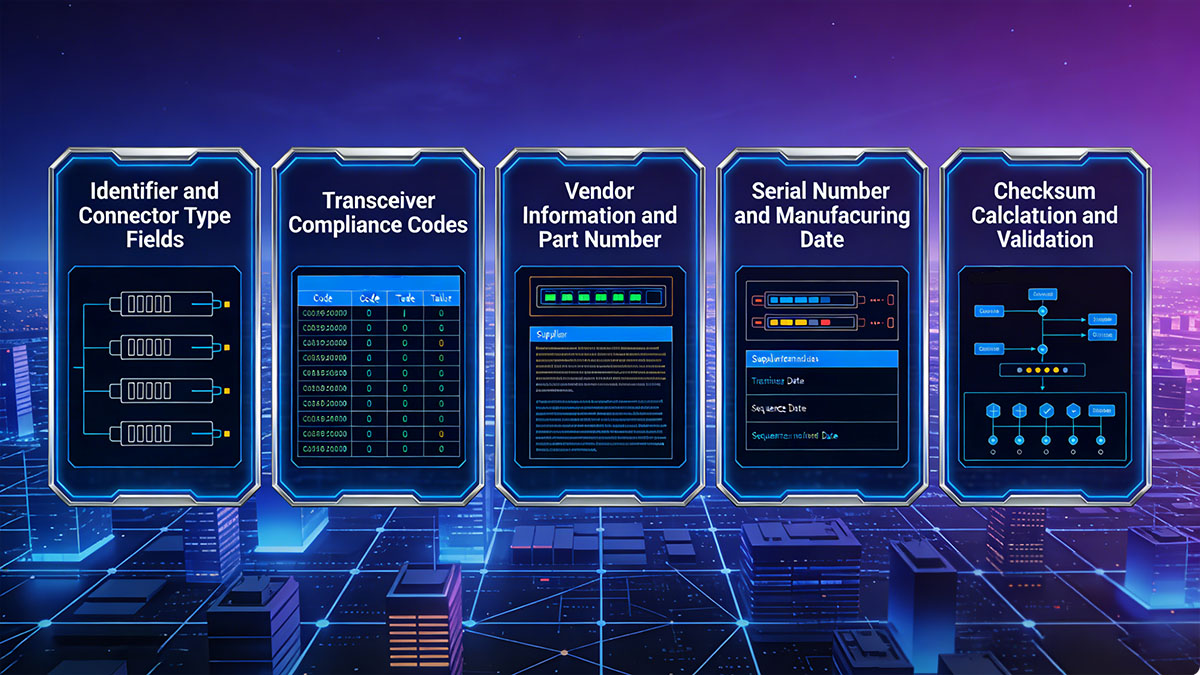
Identifier and Connector Type Fields
The first few bytes in the A0h memory map define the basic identity and physical interface of the module:
- Identifier (Byte 0): Indicates the module type (e.g., SFP/SFP+), allowing the host to recognize the form factor.
- Connector Type (Byte 2): Specifies the physical connector used, such as LC, SC, or RJ45.
- Encoding and Data Rate Fields: Provide information about signal encoding methods and supported data rates.
These fields enable the host to quickly determine how the module should be interfaced and whether it matches system requirements.
Transceiver Compliance Codes
This section defines the communication standards and protocols supported by the module. It typically spans multiple bytes, with each bit representing a specific compliance category.
- Ethernet Compliance Codes (e.g., 1000BASE-SX, 10GBASE-LR)
- Fibre Channel Compliance Codes
- SONET/SDH Compliance Codes
- Extended or Vendor-Specific Capabilities
By reading these codes, the host system can verify whether the module supports the required network standards and transmission distances.
Vendor Information and Part Number
The A0h memory map includes detailed vendor-specific identification fields that help uniquely identify the module:
- Vendor Name (Bytes 20–35): ASCII string identifying the manufacturer.
- Vendor OUI (Bytes 37–39): Organizationally Unique Identifier assigned to the vendor.
- Part Number (Bytes 40–55): Specifies the exact model of the transceiver.
- Revision Level (Bytes 56–59): Indicates the hardware or firmware revision.
These fields are essential for inventory management, compatibility checks, and vendor traceability.
Serial Number and Manufacturing Date
To support lifecycle tracking and quality control, each SFP module includes unique production information:
- Serial Number (Bytes 68–83): A unique identifier assigned to each individual module.
- Date Code (Bytes 84–91): Represents the manufacturing date, typically in YYYYMMDD format.
- Lot or Batch Information (Optional): May be included for internal tracking by the manufacturer.
This information allows operators to trace modules back to production batches, which is useful for maintenance and troubleshooting.
Checksum Calculation and Validation
To ensure data integrity, the A0h memory map includes checksum fields that validate stored data. These checksums are calculated over specific byte ranges and allow the host system to detect corruption or invalid programming.
- Base ID Checksum (Byte 63): Covers bytes 0–62 of the A0h memory space.
- Extended ID Checksum (Byte 95): Covers bytes 64–94.
- Validation Process: The host recalculates the checksum and compares it with the stored value to verify data integrity.
If a mismatch is detected, the host may flag the module as invalid or unreliable. This mechanism ensures that the SFP form factor maintains consistent and trustworthy identification data across all compliant modules.
? SFP Form Factor A2h Memory Map (Diagnostics and Monitoring)
The SFP form factor A2h memory map is dedicated to real-time diagnostics and operational monitoring, as defined by the SFF-8472 standard. Unlike the A0h area, this region contains dynamic data that reflects the current state of the module. It enables the host system to continuously monitor performance and detect abnormal conditions.

Digital Diagnostic Monitoring (DDM) Overview
Digital diagnostic monitoring (DDM) is a key feature of the A2h memory space, allowing the host to access real-time operating parameters of the SFP module. These parameters are internally measured by sensors and converted into digital values stored in predefined memory locations.
DDM provides visibility into the module’s health and performance, making it essential for network management and predictive maintenance. It also supports threshold-based alarms and warnings, enabling proactive fault detection before failures occur.
Temperature and Voltage Monitoring
The A2h memory map includes registers for monitoring internal temperature and supply voltage, which are critical for stable operation:
Temperature Measurement
- Typically stored as a 16-bit value (MSB + LSB).
- Represents internal module temperature in degrees Celsius.
- Used to detect overheating conditions.
Supply Voltage (Vcc)
- Also stored as a 16-bit value.
- Reflects the module’s operating voltage level.
- Helps identify power instability or faults.
These parameters are continuously updated and can be compared against predefined thresholds to trigger alarms or warnings.
TX Bias Current and Optical Power
In addition to environmental parameters, the A2h memory map provides insight into optical performance:
TX Bias Current
- Indicates the drive current applied to the laser.
- Helps assess laser health and aging.
TX Optical Power
- Measures the optical output power of the transmitter.
- Ensures signal strength meets required levels.
RX Optical Power
- Represents the received optical signal strength.
- Useful for detecting link degradation or fiber issues.
These values are essential for evaluating link quality and ensuring reliable data transmission.
Calibration Constants and Scaling Factors
Raw diagnostic values stored in the A2h memory map often require conversion to meaningful physical units. This is achieved using calibration constants and scaling factors defined within the module.
Internal Calibration
- The module performs conversions internally.
- Host reads already scaled values.
External Calibration
- Host applies calibration formulas using stored coefficients.
- Requires additional processing but offers flexibility.
Scaling Factors
- Define how raw ADC values map to real-world units (e.g., mA, mW, °C)
These calibration mechanisms ensure that diagnostic readings are accurate and consistent across different modules. Proper interpretation of these values is essential for effective monitoring within the SFP form factor ecosystem.
? SFP Form Factor Register Definitions and Functions
Within the SFP form factor, registers serve as the fundamental interface for accessing and controlling module behavior. Defined by the SFF-8472 standard, these registers map specific functions to fixed memory locations. They enable the host system to read status information, configure module settings, and respond to operational conditions.
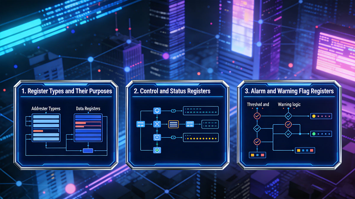
Register Types and Their Purposes
SFP registers can be broadly categorized based on their function and usage. Each type plays a distinct role in enabling communication and control:
Static Registers
- Store fixed information such as module identity and vendor data.
- Typically located in the A0h memory space.
- Read-only during normal operation.
Dynamic Registers
- Contain real-time diagnostic data (e.g., temperature, voltage).
- Continuously updated by the module.
- Located in the A2h memory space.
Control Registers
- Allow the host to configure module behavior.
- Examples include enabling/disabling transmitter or selecting modes.
Status Registers
- Reflect the current operational state of the module.
- Indicate conditions such as faults or signal loss.
Control and Status Registers
Control and status registers are essential for managing and monitoring module operation. Control registers are typically writable, allowing the host to influence module behavior, while status registers are read-only and provide feedback.
Control Registers
- Used to enable or disable features (e.g., TX_DISABLE control).
- May configure operational modes or reset conditions.
- Require careful handling to avoid unintended disruptions.
Status Registers
- Provide real-time indicators such as: TX fault condition, RX loss of signal (LOS), and module readiness.
- Help the host quickly assess link health and module state.
Together, these registers form a feedback loop where the host can both control and observe the module’s behavior in real time.
Alarm and Warning Flag Registers
Alarm and warning flag registers are used to indicate when monitored parameters exceed predefined thresholds. These registers are critical for proactive monitoring and fault management.
Alarm Flags
- Triggered when a parameter exceeds critical limits.
- Indicate conditions that may lead to failure (e.g., overheating, power out of range).
Warning Flags
- Indicate that a parameter is approaching a critical threshold.
- Provide early warning for preventive action.
Typical Monitored Parameters
- Temperature
- Supply voltage
- TX bias current
- Optical power (TX/RX)
These flags are typically implemented as bit fields within specific registers, allowing multiple conditions to be monitored simultaneously. By continuously checking these registers, the host system can respond quickly to abnormal conditions and maintain reliable operation of the SFP form factor transceiver.
? SFP Form Factor EEPROM Access and Data Integrity
The SFP form factor relies on EEPROM as the underlying storage for both identification and diagnostic data. Access to this memory is performed through the I2C interface, enabling the host to read and, in some cases, write specific data fields. Ensuring data integrity during these operations is critical for reliable module identification and monitoring.
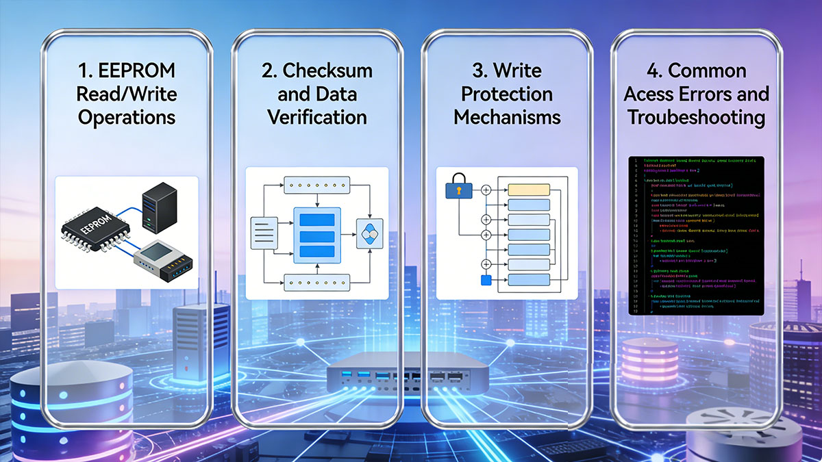
EEPROM Read/Write Operations
In typical SFP modules, EEPROM access is primarily read-focused. The host continuously reads data from the A0h and A2h memory areas to obtain identification details and real-time diagnostics. These read operations can be performed either byte-by-byte or sequentially across multiple addresses, depending on the required data.
Write operations, on the other hand, are usually restricted. Only certain locations — such as control-related bytes or page selection registers — may allow writing, and even then, strict timing and command sequences must be followed. Most identification fields remain read-only to prevent accidental or unauthorized modification, ensuring consistency across deployments.
Checksum and Data Verification
To maintain data reliability, checksum mechanisms are implemented within the EEPROM structure. Specific byte ranges — such as the base and extended identification fields — are protected by checksum values stored in designated locations.
When the host reads data, it can recalculate the checksum and compare it with the stored value. Any mismatch indicates potential data corruption or programming errors. This simple but effective validation method helps ensure that critical information, such as vendor identity and module specifications, remains accurate.
Write Protection Mechanisms
SFP modules incorporate protection mechanisms to safeguard EEPROM content. Most of the A0h memory space is permanently read-only, preserving factory-programmed identification data. In some cases, hardware-level protection prevents writes to sensitive regions entirely.
For writable areas, access may be controlled through specific registers or command sequences, limiting changes to authorized operations only. These safeguards help maintain the integrity of the SFP form factor memory map and prevent unintended disruptions.
Common Access Errors and Troubleshooting
During EEPROM communication, errors can occur due to incorrect I2C handling or misinterpretation of the memory structure. Common issues include addressing the wrong memory space (A0h vs A2h), receiving NACK responses from the module, or encountering timeouts caused by improper timing.
In practice, troubleshooting involves verifying I2C signal integrity, ensuring correct device addressing, and rechecking data using checksum validation. By following proper access procedures and understanding the memory structure, most issues can be quickly identified and resolved.
? Summary of SFP Form Factor Memory Map and Register Architecture
The SFP Form Factor memory map, defined by the SFF-8472 standard, provides a well-structured framework for accessing both static identification data and real-time diagnostics. From the A0h Serial ID information to the A2h diagnostic monitoring, each memory region and register plays a specific role in enabling interoperability, monitoring, and control. The use of a standardized I2C interface further ensures consistent communication across different devices and vendors.
By understanding the memory map structure, register definitions, and EEPROM access mechanisms, engineers and network operators can more effectively manage SFP modules, troubleshoot issues, and optimize system performance. This structured approach not only simplifies integration but also enhances reliability and scalability in modern optical networks.
If you are looking for high-quality, standards-compliant SFP transceiver modules, visit the LINK-PP Official Store to find products tailored to your networking needs.