As modern data centers push for faster networks, achieving the next level of QSFP speed has become essential for handling massive amounts of data. To reach blazing-fast 200G and 400G thresholds, the industry has shifted from traditional NRZ encoding to advanced PAM4 modulation. However, squeezing higher bandwidth out of these next-generation transceivers comes with a major catch: increased signal complexity.
Maintaining peak QSFP speed requires a deep dive into signal integrity, as higher data rates are highly sensitive to interference and loss. Challenges like insertion loss, crosstalk, and thermal drift can easily distort data packets before they reach their destination. Understanding how to manage these hardware obstacles is the ultimate key to unlocking reliable, high-performance connectivity in next-gen networks.
📝 Demystifying QSFP Speed: The Evolution from NRZ to PAM4
The demand for massive data throughput is fundamentally changing how optical transceivers transmit information. Moving beyond traditional boundaries requires a revolutionary shift in signaling technology to sustain higher data rates. Exploring this evolution reveals how hardware designs adapt to achieve unprecedented performance levels.
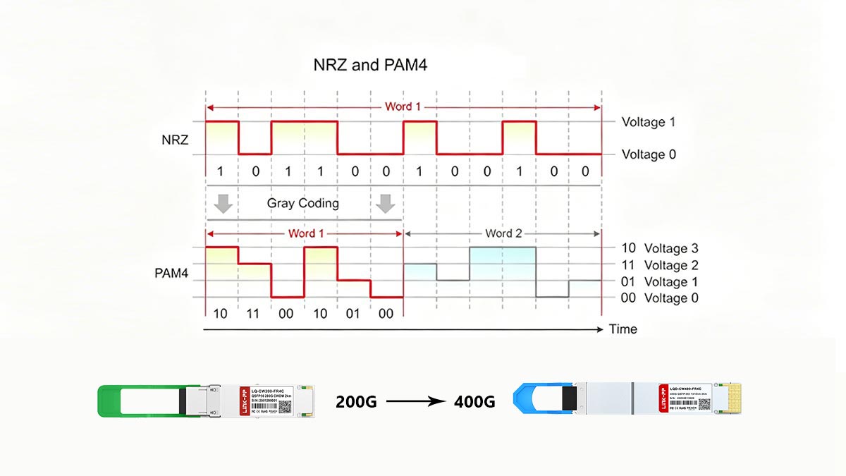
Understanding the Shift to 200G and 400G Networks
Modern data centers are facing an unprecedented explosion of cloud traffic, AI workloads, and ultra-high-definition video streaming. To prevent massive network bottlenecks, infrastructure must scale up rapidly to support 200G and 400G bandwidth demands.
Upgrading to these faster networks ensures that enterprises can handle millions of simultaneous data requests without latency. This transition relies heavily on maximizing QSFP speed through cutting-edge hardware design and advanced engineering.
Why Traditional NRZ Encoding Fails at Higher Data Rates
For decades, Non-Return-to-Zero (NRZ) encoding was the standard method for data transmission, using simple high and low voltage levels to represent 1s and 0s. However, as speeds attempt to cross into the 200G and 400G domains, NRZ requires a drastically high frequency that causes severe signal degradation over standard fiber.
At ultra-high frequencies, copper traces act like antennas, leaking energy and causing extreme signal attenuation. Consequently, continuing with NRZ would make the hardware design too expensive and physically impractical for next-generation data centers.
The Basics of PAM4 Modulation in Next-Gen Transceivers
To overcome the physical limitations of NRZ, next-generation transceivers adopt Pulse Amplitude Modulation 4-Level (PAM4) technology. Instead of using just two voltage levels, PAM4 utilizes four distinct signal levels to transmit two bits of data in the exact same time slot.
The following visual breakdown illustrates how PAM4 achieves double the data efficiency compared to traditional binary signaling methods:
| Modulation Type |
Voltage Levels |
Bits Per Symbol |
Relative Bandwidth Efficiency |
| NRZ (Binary) |
2 (High / Low) |
1 bit |
Baseline (1x) |
| PAM4 |
4 (00, 01, 10, 11) |
2 bits |
Doubled (2x) |
By packing twice as much information into each cycle, PAM4 allows network hardware to achieve maximum QSFP speed without needing to double the operating frequency.
Key Differences in Signal Complexity and Throughput
While PAM4 successfully doubles network throughput, it introduces significant complexity because it splits the signal into three distinct "eyes" instead of one. This reduction in eye height makes the signal much more vulnerable to noise and minor electrical interference.
As a result, designers must implement advanced error correction and high-quality components to clean up the signal. Balancing this increased complexity against the massive boost in throughput is the core challenge of modern high-speed link design.
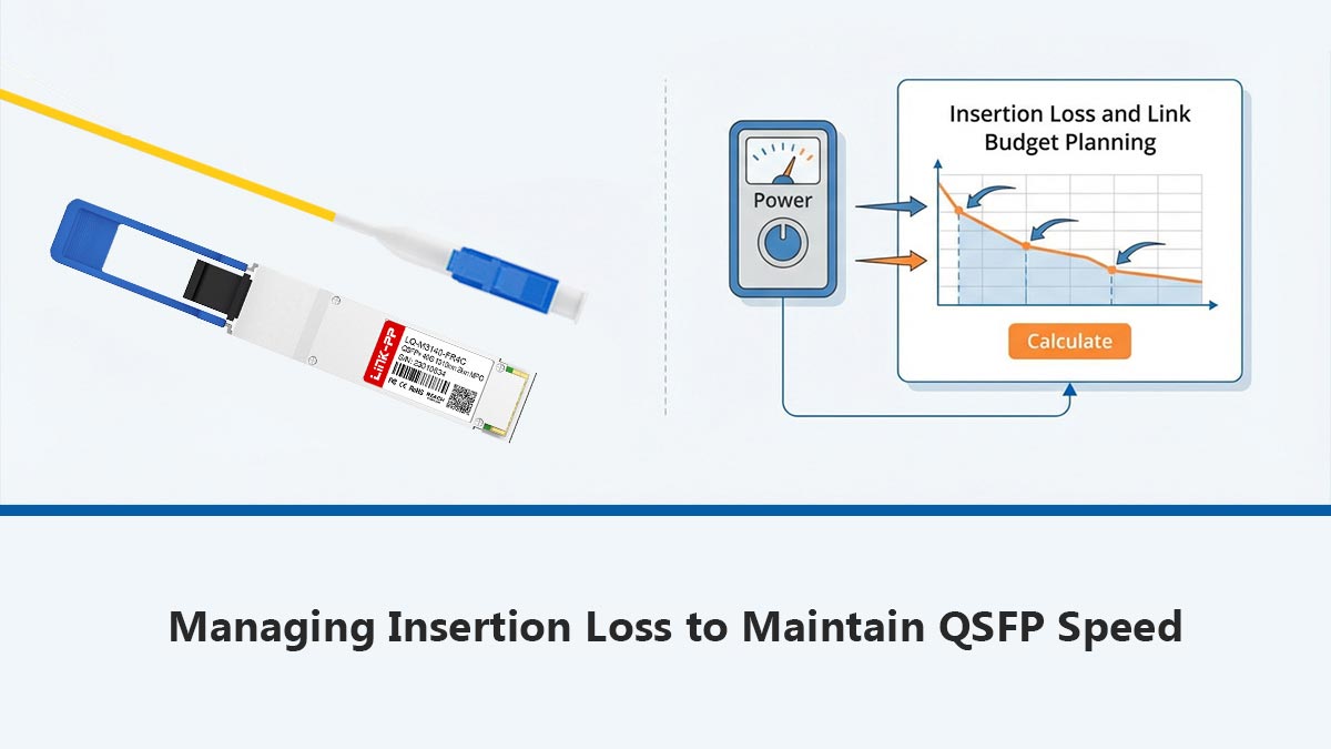
📝 Managing Insertion Loss to Maintain QSFP Speed
As QSFP speed climbs to extreme frequencies, signal energy naturally dissipates when traveling through a network channel. Left unchecked, this drop in signal power can degrade performance and lead to critical data corruption. Proactively managing insertion loss ensures that high-speed links operate efficiently and maintain consistent data transmission.
What Causes Signal Attenuation in High-Speed Fiber Links
When light travels through fiber optic cables, it naturally encounters physical forces that reduce its overall strength. This loss of signal amplitude can weaken the data stream before it reaches its destination transceiver.
The primary culprits behind this optical signal degradation include the following factors:
- Material absorption: Glass fibers absorb tiny amounts of light energy.
- Rayleigh scattering: Microscopic structural variations deflect light waves.
- Macrobending and microbending: Tight cable twists leak light out of the core.
- Splice and connection points: Imperfect alignments scatter incoming light.
Maximum Allowable Loss Budgets for 200G/400G Links
High-speed 200G and 400G networks operate under incredibly strict loss margins due to the fragile nature of PAM4 signals. If the total channel loss exceeds a specific threshold, the receiver will fail to accurately decode the four distinct voltage levels.
Engineers rely on strict guidelines to calculate and maintain a stable network link budget:
- IEEE standard compliance: Links must adhere to tight dB limits.
- Allocation for margins: Budgets must include safety buffers for component aging.
- Distance limitations: Maximum reach decreases as data speed scales up.
- Total channel calculation: Designers must sum up fiber, connector, and splice losses.
Best Practices for Minimizing PCB Trace Losses
Inside the networking equipment, high-speed signals must travel across circuit boards before reaching the optical modules. Traditional PCB materials tend to absorb high-frequency electrical signals, severely hindering optimal hardware performance.
Implementing smart PCB design strategies helps preserve signal integrity over short distances:
- Low-loss dielectrics: Use high-grade materials like Megtron 6 or Megtron 7.
- Smooth copper foils: Choose ultra-low profile copper to reduce skin-effect loss.
- Shorter trace routing: Keep the physical path between chips and transceivers minimal.
- Avoiding vias: Limit the use of vertical board transitions to prevent impedance changes.
How High-Quality Connectors Preserve Signal Strength
The interface where the QSFP module plugs into the switch cage represents a critical point for potential signal reflection and loss. Any mechanical misalignment at this junction can create massive barriers for ultra-fast PAM4 waves.
Using premium, precision-engineered connectors offers vital hardware benefits for high-speed channels:
- Impedance matching: Connectors maintain a steady 100-ohm differential path.
- Minimized insertion force: High-quality pins prevent physical wear over time.
- Enhanced shielding: Advanced metal cages block external electromagnetic interference.
- Precise mechanical alignment: Tight tolerances maximize optical core-to-core contact.
📝 Combating Inter-Symbol Interference (ISI) at Maximum QSFP Speed
At ultra-high data rates, consecutive data pulses can easily bleed into one another, creating a phenomenon known as Inter-Symbol Interference (ISI). This blurring of signals makes it incredibly difficult for the receiving QSFP transceiver to distinguish where one bit ends and the next begins. Overcoming ISI requires a combination of smart hardware design and sophisticated digital signal processing to keep data moving accurately.
The Physics Behind Reflection and Reflection-Induced Noise
When a high-speed electrical signal encounters an abrupt change in impedance along its path, a portion of its energy bounces backward toward the source. These reflections travel back and forth within the copper traces, colliding with incoming data pulses and creating reflection-induced noise.
This chaotic bouncing of energy severely distorts the voltage levels of the channel. For PAM4 signals, which rely on precise voltage thresholds, even minor reflection noise can completely close the signal eyes and corrupt the data stream.
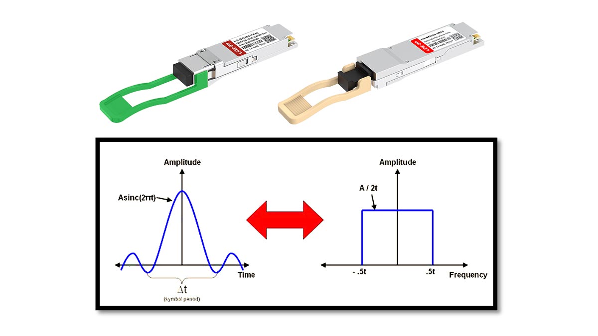
How High Baud Rates Amplify Channel Distortion
To achieve maximum QSFP speed, next-generation networks utilize incredibly high baud rates, meaning symbols are transmitted much closer together in time. Because the duration of each symbol is extremely short, the signal becomes highly vulnerable to the physical imperfections of the transmission line.
As these tightly packed symbols travel down the channel, any residual energy from a previous pulse can spill directly into the time slot of the following pulse. This cumulative distortion stretches the signal waves out of shape, making severe channel degradation inevitable without active intervention.
Utilizing Adaptive Equalization Techniques (CTLE and DFE)
To repair the signal distortion caused by ISI, modern transceivers utilize advanced adaptive equalization techniques directly inside the silicon chips. Continuous-Time Linear Equalization (CTLE) works at the front end to boost high-frequency components while filtering out low-frequency noise.
Following CTLE, Decision Feedback Equalization (DFE) takes over to dynamically cancel out the remaining ISI based on the history of previously received symbols. Working together, this powerful pair flattens out the channel response and reopens the closed PAM4 eyes for accurate decoding.
Clock and Data Recovery (CDR) Strategies for PAM4
Clock and Data Recovery (CDR) circuits act as the heartbeat of the receiving module, precisely timing when to sample the incoming data. With PAM4 modulation, the CDR must find the exact center of three distinct eye diagrams simultaneously amidst heavy noise.
Next-gen transceivers utilize highly advanced digital CDR architectures to lock onto the signal's timing phase with extreme precision. By maintaining a stable timing lock, the system minimizes phase jitter and ensures reliable performance at maximum throughput.
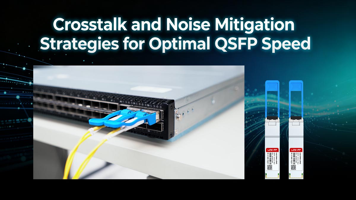
📝 Crosstalk and Noise Mitigation Strategies for Optimal QSFP Speed
In high-density networking environments, closely packed signal lines can easily leak electromagnetic energy into neighboring channels. This unwanted interference, known as crosstalk, rapidly degrades the signal-to-noise ratio required for stable PAM4 operations. Effectively suppressing this noise is vital to preventing data corruption and achieving optimal hardware throughput.
Differentiating Between Near-End (NEXT) and Far-End (FEXT) Crosstalk
Crosstalk occurs when the electromagnetic field of an "aggressor" trace disrupts the signal on a parallel "victim" trace. Depending on where this interference is measured relative to the transmitting source, it is classified as either Near-End Crosstalk (NEXT) or Far-End Crosstalk (FEXT).
The following comparison table details the fundamental behavioral differences between these two primary forms of network interference:
| Crosstalk Type |
Measurement Location |
Behavior with Distance |
Impact on High-Speed Links |
| Near-End (NEXT) |
Near the transmitting source |
Remains strong, independent of length |
Highly disruptive; can overpower weak incoming signals |
| Far-End (FEXT) |
At the far end of the channel |
Attenuates along with the line length |
Highly dependent on channel layout and trace length |
Understanding these distinct noise vectors allows hardware engineers to apply targeted suppression techniques at both ends of the transmission line.
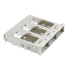
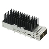
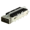
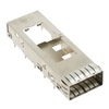
Shielding Techniques in High-Density QSFP-DD Form Factors
The compact QSFP-DD form factor packs eight high-speed electrical lanes into a single, tightly constrained physical housing. To prevent these lanes from constantly interfering with one another, advanced mechanical shielding must be integrated directly into the connector cage.
Manufacturers utilize precision-engineered metal gaskets and specialized internal grounding tabs to isolate individual transmit and receive channels. This multi-layered structural shielding blocks stray electromagnetic waves from bleeding into adjacent ports on high-density network switches.
Optimizing PCB Layout Design for Trace Isolation
Inside the network equipment, proper circuit board layout serves as the first line of defense against severe signal degradation. Layout designers must maintain strict spacing rules, often adhering to the "3W rule," which dictates that the distance between traces must be three times their width.
Additionally, embedding high-speed differential pairs into the inner layers of the PCB — sandwiched securely between solid ground planes — provides excellent isolation. This routing strategy significantly reduces electromagnetic fields and minimizes trace-to-trace noise coupling.
The Impact of Power Supply Noise on Transceiver Performance
High-speed optical transceiver modules rely on an exceptionally stable direct current (DC) power delivery network to drive internal laser components. If voltage ripples or switching noise from the main power supply leak into the module, they can cause immediate signal instability.
This power-induced noise directly translates into increased jitter and fluctuating laser driver amplitudes, which can collapse the fragile PAM4 eye diagram. Implementing robust decoupling capacitors right next to the QSFP power pins is critical for filtering out these unwanted high-frequency ripples.
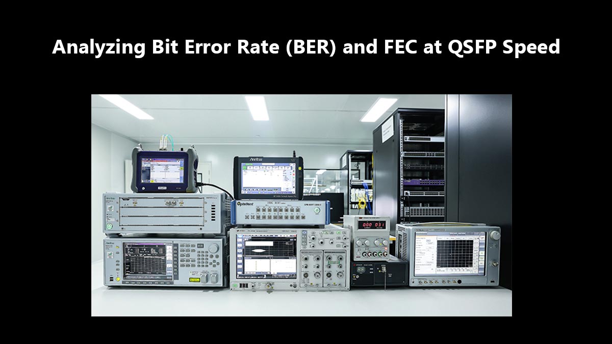
📝 Analyzing Bit Error Rate (BER) and FEC at QSFP Speed
Evaluating how often data packets become corrupted is essential for maintaining dependable network performance at higher bandwidths. Because ultra-fast data transmissions are highly sensitive to electrical noise, tracking bit errors provides a direct look into the overall health of the physical link. Managing these errors through specialized algorithms ensures that enterprise hardware achieves its maximum throughput without sacrificing data accuracy.
Why PAM4 Links Inherently Operate with a Higher Native BER
Compared to traditional NRZ encoding, PAM4 utilizes four distinct voltage levels packed closely together within the same physical amplitude space. This tight spacing cuts the available signal-to-noise ratio by one-third, making it much harder for the receiver to distinguish between different values. As a direct result, minor electrical fluctuations or ambient noise frequently cause the system to misinterpret the transmitted bits.
Because of this reduced signal margin, next-generation networks naturally operate with a much higher raw, or "native," error rate right out of the box. Hardware designers accept this compromise because the technology offers double the throughput capacity of older, less complex signaling methods. Consequently, managing this inherent noise floor requires integrated mathematical tools to clean up the data stream before it reaches its final destination.
The Essential Role of Forward Error Correction (FEC) in 200G/400G Architecture
Forward Error Correction (FEC) serves as a critical safety net by adding structured mathematical redundancy directly into the transmitted data stream. When the receiving transceiver catches bit errors caused by channel noise, the integrated FEC algorithm detects and instantly repairs those flipped bits on the fly. This real-time correction occurs without requiring the destination switch to request a time-consuming retransmission of the corrupted packet.
Without the protective layer of FEC, a 200G or 400G QSFP link would suffer from constant packet drops and severe application latency. The algorithm successfully transforms a noisy, error-prone raw signal into a pristine, highly reliable connection suitable for mission-critical enterprise environments. Therefore, integrating advanced FEC processing is a non-negotiable requirement for unlocking stable performance at maximum hardware speeds.
Real-Time Pre-FEC BER Monitoring vs. Post-FEC Performance
Network administrators constantly evaluate link health by comparing the raw data error rate before and after the correction algorithm does its work. Pre-FEC BER measures the exact number of raw errors introduced by the physical fiber, connectors, and circuit boards. Tracking this baseline metric acts as an early warning system, highlighting gradual hardware degradation or dirty optical interfaces before a catastrophic failure occurs.
In contrast, Post-FEC Performance represents the actual error rate delivered to the networking operating system after all corrections are finished. In a healthy deployment, even a highly distorted link with a high Pre-FEC BER can achieve a virtually flawless Post-FEC score. Monitoring the widening gap between these two metrics gives engineers clear visibility into how hard the error correction engine is working to maintain stability.
Setting Acceptance Thresholds for Reliable Optical Links
To guarantee long-term network uptime, engineering standards define very strict maximum limits for acceptable bit error rates before the link drops entirely. If the raw Pre-FEC error rate crosses a specific mathematical boundary, the FEC engine becomes overwhelmed and can no longer correct the incoming data. For most standard 400G links, the industry-accepted threshold requires the raw error rate to stay well below 2.4×10⁻⁴ to ensure flawless recovery.
When a transceiver detects that its error rates are creeping dangerously close to these pre-defined limits, it triggers automated system alerts. Network management software can then proactively reroute traffic or flag the specific optical module for physical inspection and cleaning. Adhering to these strict baseline thresholds prevents unexpected network blackouts and keeps data flowing smoothly across the infrastructure.
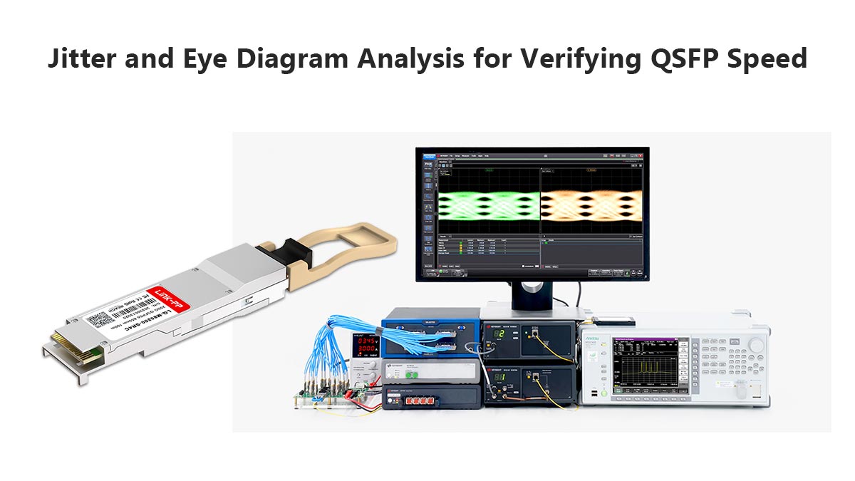
📝 Jitter and Eye Diagram Analysis for Verifying QSFP Speed
Testing engineers use eye diagrams and jitter analysis to confirm that high-speed network components are working correctly. These visual tools show the physical quality of the electrical and optical signals as they travel through the hardware. Analyzing these measurements ensures that the system maintains optimal data performance without signal breakdown.
Decoding the Four-Level PAM4 Eye Diagram
An eye diagram is formed by overlapping multiple signal waveforms on a test screen to display data transitions. While older NRZ technology creates a single open eye pattern, PAM4 technology displays three distinct eyes stacked vertically. These three openings represent the transitions between the four different voltage levels used to transmit data.
Testing engineers inspect these openings to check the overall quality and clarity of the high-speed transmission. If the signal suffers from heavy noise, the three openings will appear blurry or completely closed. A clean and wide-open triple-eye pattern indicates that the transceiver can successfully read all incoming bits.
Understanding Deterministic vs. Random Jitter in 200G/400G Links
Jitter refers to the unwanted variations in the timing of a signal pulse, which can cause data errors. Deterministic jitter is caused by predictable hardware factors such as circuit board design flaws or reflections. Because this type of timing error has specific physical causes, engineers can identify and fix it by improving the circuit layout.
Random jitter is caused by unpredictable thermal noise and natural physical variations within the electronic components. Unlike deterministic jitter, random errors follow a statistical pattern and cannot be completely removed from the system. Minimizing both types of timing variations is necessary to prevent data corruption at fast transmission rates.
Measuring Eye Width and Eye Height for Signal Validation
Eye height measures the vertical opening of the signal pattern, which indicates the noise margin of the link. If the eye height is too small, the receiver cannot accurately tell the difference between the voltage steps. Measuring this vertical space helps engineers confirm that the signal is strong enough to resist basic electrical interference.
Eye width measures the horizontal opening, which represents the time available for the receiver to sample the data. Narrow eye widths indicate that timing variations are shifting the data pulses out of their proper position. Systems must meet specific height and width standards to ensure that the network hardware functions reliably over time.
Essential Test Equipment for Troubleshooting High-Speed Jitter
Engineers use specialized high-bandwidth digital sampling oscilloscopes to capture and display these complex PAM4 eye diagrams. These instruments must have exceptionally low internal noise to avoid adding artificial errors to the measurements. The oscilloscope separates the different types of jitter so that technicians can locate the exact source of a problem.
Additionally, bit error rate testers (BERTs) are connected to the network to send and verify known data patterns. By running these testers alongside the oscilloscope, engineers can match physical signal distortions directly to specific data loss events. Using this advanced equipment is the standard way to verify that a hardware system is ready for live deployment.
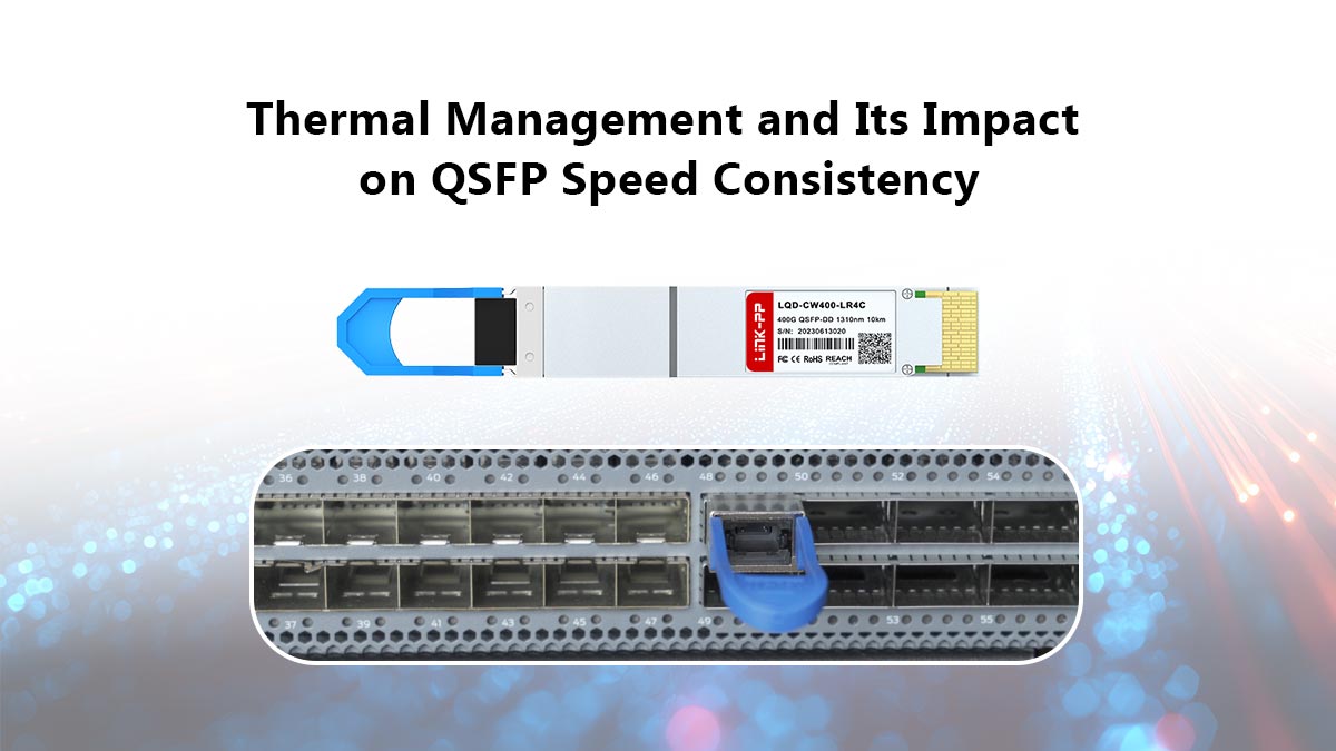
📝 Thermal Management and Its Impact on QSFP Speed Consistency
High-speed optical transceivers generate a significant amount of heat during continuous data transmission. If this heat is not removed quickly, the temperature rise can degrade the performance of internal electronic components. Implementing effective cooling strategies is essential to keep the system running reliably and at a constant speed.
How Heat Dissipation Affects Laser Diode Efficiency
The internal laser diode relies on a stable temperature to emit light waves at the correct wavelength. When heat builds up inside the optical module, it reduces the efficiency of light production and lowers the overall output power. This reduction in optical power directly shrinks the signal margins, which makes data transmission more vulnerable to background noise.
The primary consequences of unmanaged laser heat include the following operational issues:
- Wavelength shifting: Optical frequencies drift away from standard channels.
- Reduced light output: The signal becomes too dim for long distances.
- Increased noise floor: Extra electrical distortion enters the laser driver.
- Accelerated aging: Internal semiconductor parts wear out much faster.
Thermal Challenges of Dense 200G/400G QSFP-DD Optical Modules
The QSFP-DD form factor packs eight parallel data lanes into a single compact housing. Because these modules operate at extreme speeds, their internal chips consume a large amount of power and produce intense heat. Cooling these modules is difficult because the tight physical spacing inside modern switch cages limits natural airflow.
Engineers must manage several severe thermal complications caused by this high-density layout:
- Hot spots: Intense heat concentrates in tiny areas on the chip.
- Thermal coupling: Heat leaks from one module into neighboring ports.
- Airflow resistance: Dense connector cages block the cooling air path.
- Component stress: High temperatures cause internal micro-expansions.
Passive vs. Active Cooling Designs in Enterprise Switches
Data center equipment relies on different physical cooling mechanisms to remove heat from the optical ports. Passive cooling methods use metal heat sinks attached to the module cage to pull heat away without using power. Active cooling systems use motorized chassis fans to force high-speed air across these heat sinks to accelerate cooling.
Choosing the right cooling method depends on the specific hardware design and power limits:
- Passive heat sinks: Use copper riding chips to absorb static heat.
- Variable fan speeds: Increase chassis airflow as internal temperatures rise.
- Airflow direction: Pull cool air from the front to exhaust out the back.
- Thermal interface materials: Use specialized pads to improve heat transfer.
Monitoring Temperature Thresholds to Prevent Signal Drift
Modern network operating systems constantly track the internal temperature sensors embedded inside each optical module. If a transceiver crosses a pre-defined temperature threshold, the system can take immediate action to protect the hardware. This real-time monitoring prevents sudden component failures and maintains consistent transmission characteristics.
Automated network systems respond to temperature variations through several protective steps:
- Warning alerts: Software flags modules that exceed safe operational limits.
- Dynamic adjustments: Internal laser drivers modify bias currents to compensate.
- Traffic rerouting: Switches shift critical data paths away from hot ports.
- Emergency shutdown: System cuts power to modules facing thermal destruction.
📝 Conclusion: Achieving Reliable Signal Integrity at Maximum QSFP Speed

Achieving maximum data performance in 200G and 400G networks requires a complete understanding of physical signal limitations. Engineers must balance advanced PAM4 modulation against real-world hardware challenges like insertion loss, crosstalk, and thermal dissipation. Addressing these issues with precise PCB layouts, advanced equalization, and active cooling ensures that your infrastructure remains stable and efficient.
Investing in premium, high-quality hardware components is the most effective way to eliminate data errors and maintain constant connection uptime. Using reliable transceivers designed for strict signal standards prevents unexpected data loss and protects your network investment over time. To find dependable, high-performance QSFP optical modules optimized for next-generation systems, explore the premium options available at the LINK-PP Official Store.